Eureka AIR delivers breakthrough ideas for toughest innovation challenges, trusted by R&D personnel around the world.

Organic transistor

a transistor and organic technology, applied in the field of organic transistors, can solve the problems of weak pentacene adhesion to the substrate, low electric charge transfer speed of the tft proposed by j. drury et al., and the semiconductor material has seldom attracted attention for practical applications, etc., and achieves high power handling capability, high operating speed, and low cost.

Inactive Publication Date: 2006-11-02
RICOH KK
View PDF15 Cites 14 Cited by
  • Summary
  • Abstract
  • Description
  • Claims
  • Application Information

AI Technical Summary

Benefits of technology

[0014] Accordingly, a general object of the present invention is to provide a low cost organic transistor that provides a high speed operation and a high power capability, and another and more specific object of the present invention is to provide a low cost organic EL transistor that provides a high speed operation, a high power capability, and a high luminous efficiency, which substantially obviates one or more of the problems caused by the limitations and disadvantages of the related art.
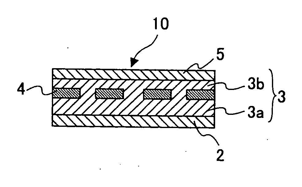
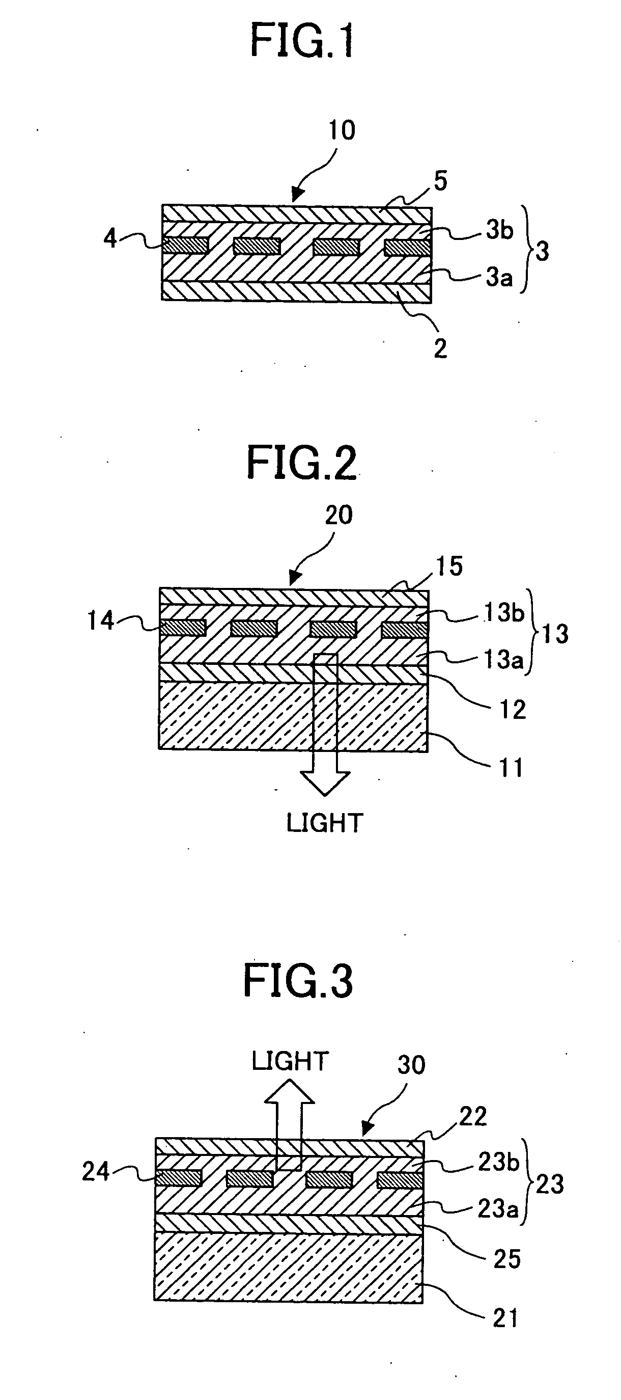
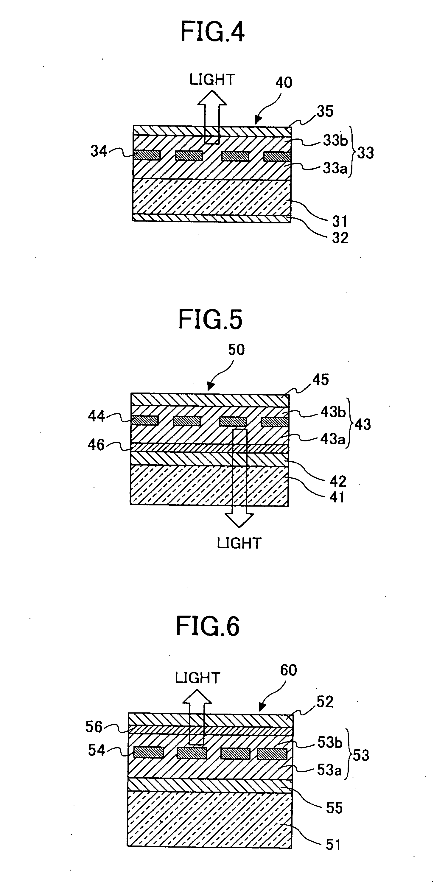
[0017] The inventors of the present invention have found that an organic transistor as structured below provides a high operating speed, a high power handling capability, can be manufactured at low cost, and therefore come to complete the present invention. The organic transistor includes a source electrode and a drain electrode that are prepared face to face, an organic semiconductor layer between the source electrode and the drain electrode, and gate electrodes that are shaped like a comb or a mesh, and are provided at intervals from each other approximately in a central part of the organic semiconductor layer, and approximately parallel to the source electrode and the drain electrode. Then, an electric field luminescent organic semiconductor material is used as the organic semiconductor layer, resulting in an organic EL transistor with a high operating speed, high luminescence efficiency, and a high power handling capability, which can be manufactured at a low cost.

Problems solved by technology

However, because an organic semiconductor material as above has lower electric charge transfer speed and higher resistance than an inorganic semiconductor material, the organic semiconductor material has seldom attracted attention for practical applications.
TFT formed with pentacene has shown problems in that vacuum membrane formation is required to form pentacene into a thin film, and that adhesion of pentacene to a substrate is weak.
However, the electric charge transfer speed attained by the TFT proposed by J. Drury et al. is still low, and improvements are desired.
However, a problem is that the electric charge transfer speed is low because the ordered arrangement is not available.
Thus, an organic semiconductor material that has sufficiently high electric charge transfer speed has not been found.
As mentioned above, while an organic semiconductor material offers a possibility that TFT will be realizable with cheaper and easier membrane formation technology, such as vacuum evaporation, spin-coating, dip-coating, printing, and ink jetting, which is an advantage, there is a problem in that the electric charge transfer speed is lower than desired.
Under the state of the art as described, even if TFT having an electric field effect transistor (FET) structure is simply employed as a driving unit of an organic EL element, the electric charge transfer speed is still low, and it is difficult to obtain a desired operation speed at desired power consumption.
Problems with this SIT are that: since all the films are formed by the vacuum evaporation method, costs of production equipment becomes high, and, therefore, productivity becomes low; and because the process includes exposure to the atmosphere for oxidizing the metal, control is difficult, and reproducibility is not satisfactory.

Method used


Image

  • Organic transistor
  • Organic transistor
  • Organic transistor

Examples


embodiment 1

[0063] (a) The drain electrode that is 1 micrometer thick was formed on the upper surface of a transparent glass substrate by sputtering a transparent electrode material consisting of ITO.

[0064] (b) A poly phenylenevinylene (PPV) solution, having viscosity of 20 CP, was prepared by dissolving PPV in a solvent consisting of xylene or chloroform, and the PPV solution was applied to the upper surface of the drain electrode by spin coating at a rotation speed of 500 rpm, such that a thin film that is about 1000 A thick was formed, which serves as a part of the (p-type) organic semiconductor layer.

[0065] (c) On the upper surface of this organic semiconductor layer, an aluminum thin film was formed by vacuum evaporation of aluminum, and comb-like gate electrodes were formed, using a metal mask formed in the comb shape.

[0066] (d) To the upper surface of the organic semiconductor layer and the comb-like gate electrodes, a spin coating of the PPV solution prepared in (b) above was perform...

embodiment 2

[0068] (a) The source electrode that is 1 micrometer thick was formed on the upper surface of a glass substrate by vacuum evaporation of an electrode material consisting of aluminum.

[0069] (b) A poly phenylenevinylene (PPV) solution, having viscosity of 20 CP, was prepared by dissolving PPV in a solvent consisting of xylene or chloroform, and the PPV solution was applied to the upper surface of the source electrode by spin coating at a rotation speed of 500 rpm, such that a thin film that is about 1000 A thick was formed, which serves as a part of the (p-type) organic semiconductor layer.

[0070] (c) On the upper surface of this organic semiconductor layer, an aluminum thin film was formed by vacuum evaporation of aluminum, and the comb-like gate electrodes were formed, using a metal mask formed in the comb shape.

[0071] (d) To the upper surface of the organic semiconductor layer and the comb-like gate electrodes, a spin coating of the PPV solution prepared in (b) above was performe...

embodiment 3

[0073] (a) The drain electrode that is 1 micrometer thick was formed on the back surface of a Si substrate that was highly doped with boron (B) or phosphor (P), having a low resistance characteristic, by vacuum evaporation of an electrode material consisting of aluminum.

[0074] (b) A poly phenylenevinylene (PPV) solution, having viscosity of 20 CP, was prepared by dissolving PPV in a solvent consisting of xylene or chloroform, and the PPV solution was applied to the upper surface of the Si substrate by spin coating at a rotation speed of 500 rpm, such that a thin film that is about 1000 A thick was formed, which serves as a part of the (n-type) organic semiconductor layer.

[0075] (c) On the upper surface of this organic semiconductor layer, an aluminum thin film was formed by vacuum evaporation of aluminum, and the comb-like gate electrodes were formed, using a metal mask formed in the comb shape.

[0076] (d) To the upper surface of the organic semiconductor layer and the comb-like g...


PUM

PropertyMeasurementUnit
thicknessaaaaaaaaaa
thicknessaaaaaaaaaa
thicknessaaaaaaaaaa

Abstract

An organic transistor is capable of emitting light at high luminescence efficiency, operating at high speed, handling large electric power, and can be manufactured at low cost. The organic transistor includes an organic semiconductor layer between a source electrode and a drain electrode, and gate electrodes shaped like a comb or a mesh, which are provided at intervals approximately in the central part of the organic semiconductor layer approximately parallel to the source electrode and the drain electrode. The organic semiconductor layer consists of an electric field luminescent organic semiconductor material such as compounds of naphthalene, anthracene, tetracene, pentacene, hexacene, a phthalocyanine system compound, an azo system compound, a perylene system compound, a triphenylmethane compound, a stilbene compound, poly N-vinyl carbazole, and poly vinyl pyrene.

Description

BACKGROUND OF THE INVENTION [0001] 1. Field of the Invention [0002] The present invention generally relates to an organic transistor, and especially relates to an organic electro luminescent (EL) transistor that is useful as a self-luminous organic EL display, and capable of switching and luminescence functions by combining an organic light emitting diode (LED) and an organic transistor. [0003] 2. Description of the Related Art [0004] In recent years, research has actively been carried out about organic EL elements because it has become clear that the organic EL elements are superior to luminous devices that deploy inorganic materials for reasons such as (1) a lightweight structure can be provided, (2) a wide area display can be easily obtained, and (3) various luminescences can be obtained. An organic EL display using an organic EL element provides high luminosity with a thin shaped configuration and a fast response speed, and is therefore considered to be a promising next-generati...

Claims


Application Information

Patent Timeline
Patent Type & Authority Applications(United States)
IPC IPC(8): H01L29/08G09F9/30H05B33/26H01L27/28H01L27/32H01L35/24H01L51/00H01L51/05H01L51/30H01L51/50H01L51/52H05B33/12
CPCH01L51/0037H01L51/0038H01L51/5203H01L51/52H01L51/0508H10K85/114H10K85/1135H10K10/46H10K59/805H10K50/80H10K50/805
Inventor IECHI, HIROYUKIAKIYAMA, YOSHIKAZUKONDOH, HIROSHITANO, TAKANORI
Owner RICOH KK
Why Eureka
Eureka Blog
Learn More