Growth of ordered crystalline organic films

a crystalline organic film and growth technology, applied in the field of organic photosensitive films, can solve the problems of not providing power to circuitry, devices or equipment, and inherently incapable of exceeding the product's maximum total power generated by a pv devi

Active Publication Date: 2009-07-02
RGT UNIV OF MICHIGAN
View PDF9 Cites 13 Cited by
  • Summary
  • Abstract
  • Description
  • Claims
  • Application Information

AI Technical Summary

Benefits of technology

[0014]Organic PV cells have many potential advantages when compared to traditional silicon-based devices. Organic PV cells are lightweight, economical in materials use, and can be deposited on low cost substrates, such as flexible plastic foils.
[0024]However, the absorption efficiency of bulk heterojunctions are spatially limited. In general, the absorption characteristics of a heterojunction are maximized by selecting donor materials and acceptor materials with different absorption spectra. If an incident photon has a wavelength near an absorption peak of the first material but not the second material, and the incident photon transits through the bulk heterojunction predominantly via the second material (e.g., passing down the length of a “finger” of the second material), there is a reduced likelihood that the photon will contribute to photocurrent.
[0025]Thus, it would be beneficial to retain the advantages of an ordered bulk heterojunction, such as the short distances for excitons to travel before disassociation, while further increasing photon-to-exciton conversion by increasing the donor-acceptor interface area where excitons disassociate and overall layer thickness.
[0026]One means to addressing the low mobility of charge carriers in disordered organic films is to deploy processing approaches that create order and crystallinity in the organic materials. U.S. patent application Ser. No. 11 / 880,210 incorporated herein by reference, provides one such means, providing a PV cell in which the active layer is comprised of nanocrystalline organic regions forming high conductivity networks for charge extraction. This cell retains many of the benefits imparted by the use of crystalline materials, including lowered resistance, combined with the high surface area of bulk heterojunctions.SUMMARY OF THE INVENTION

Problems solved by technology

As a general rule, a photovoltaic cell provides power to a circuit, device or equipment, but does not provide a signal or current to control detection circuitry, or the output of information from the detection circuitry.
In contrast, a photodetector or photoconductor provides a signal or current to control detection circuitry, or the output of information from the detection circuitry but does not provide power to the circuitry, device or equipment.
The maximum total power generated by a PV device is inherently incapable of exceeding the product, ISC×VOC.
However, efficient crystalline-based devices, especially of large surface area, are difficult and expensive to produce due to the problems inherent in producing large crystals without significant efficiency-degrading defects.
On the other hand, high efficiency amorphous silicon devices still suffer from problems with stability.
Despite the many advantages of organic PV devices, they typically have relatively low external quantum efficiency, on the order of 1% or less.
However, this type of cell has a disadvantage in that the diffusion length (LD) of an exciton is typically much less (LD˜50 Å) than the optical absorption length (˜500 Å), requiring a trade off between using a thick, and therefore resistive, cell with multiple or highly folded interfaces, or a thin cell with a low optical absorption efficiency.
The high series resistance of these bulk heterojunction amorphous organic blends limits the active layer thickness, leading to reduced light absorption, while exhibiting low fill factor and hence low solar energy conversion efficiency.
However, the absorption efficiency of bulk heterojunctions are spatially limited.

Method used


Image

  • Growth of ordered crystalline organic films
  • Growth of ordered crystalline organic films
  • Growth of ordered crystalline organic films

Examples


examples

[0078]Specific examples of the invention are illustrated and / or described herein. However, it will be appreciated that modifications and variations of the invention are covered by the above teachings and within the purview of the appended claims without departing from the spirit and scope of the invention.

General OVPD Process

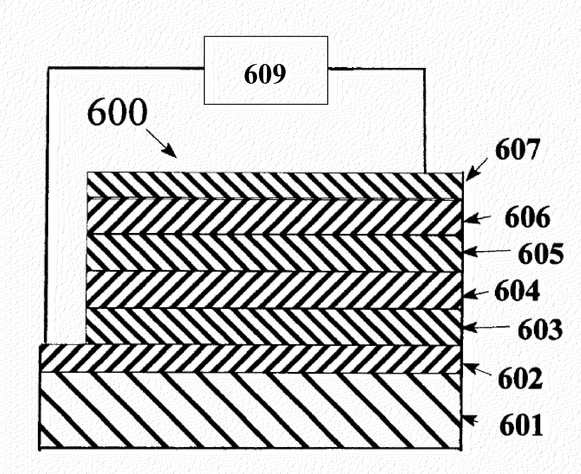
[0079]A non-limiting example of an OVPD system schematic is shown in FIG. 3. In OVPD a hot inert carrier gas 1 is infused with an evaporated organic 2 which emanates from source cell 3. The organic 2 is transported to a cooled substrate 4 where deposition occurs, thus forming film 5. Gas temperature, substrate temperature, and gas pressure can be varied to affect the crystallinity of film 5.

[0080]In one embodiment, in situ diagnostics can be used to monitor the crystallinity of the film 5, such as reflection high energy electron diffraction (RHEED), a technique which is commonly used in ultrahigh vacuum systems such as organic molecular beam deposition (OMBD).

[0...


PUM

PropertyMeasurementUnit
temperatureaaaaaaaaaa
external quantum efficiencyaaaaaaaaaa

Abstract

There is disclosed methods utilizing organic vapor phase deposition for growing bulk organic crystalline layers for organic photosensitive devices, heterojunctions and films made by such methods, and devices using such heterojunctions. There is also disclosed new methods for manufacturing heterojunctions and organic photosensitive devices, and the heterojunctions and devices manufactured thereby.

Description

CROSS REFERENCE TO PROVISIONAL APPLICATION[0001]This application claims the benefit of U.S. provisional application No. 60 / 957,902 filed Aug. 24, 2007, the disclosure of which is incorporated herein by reference.[0002]This invention was made with U.S. Government support under Contract No. FA9550-07-1-0364 awarded by the Air Force Office of Scientific Research. The government has certain rights in this invention.[0003]The present invention generally relates to organic photosensitive films for use in electronic devices, to processes for manufacturing such films, and to devices using such films.[0004]Optoelectronic devices rely on the optical and electronic properties of materials to either produce or detect electromagnetic radiation electronically or to generate electricity from ambient electromagnetic radiation.[0005]Photosensitive optoelectronic devices convert electromagnetic radiation into electricity. Solar cells, also called photovoltaic (PV) devices, are a type of photosensitiv...

Claims


Application Information

Patent Timeline
Patent Type & Authority Applications(United States)
IPC IPC(8): H01L51/46H01L51/48H01L31/0256
CPCB82Y10/00H01L51/0008H01L51/0013Y02E10/549H01L51/0053H01L51/424H01L51/0046C23C14/12C23C14/228H10K71/16H10K71/18H10K85/211H10K85/621H10K30/20H10K71/00H10K85/311
Inventor FORREST, STEPHEN R.LUNT, RICHARD R.
Owner RGT UNIV OF MICHIGAN
Why Eureka
Try Eureka