Semiconductor device with resistor elements formed on insulating film
a technology of resistor elements and semiconductor devices, applied in semiconductor devices, semiconductor/solid-state device details, diodes, etc., to achieve the effect of improving reliability and enhancing resistance value precision
- Summary
- Abstract
- Description
- Claims
- Application Information
AI Technical Summary
Benefits of technology
Problems solved by technology
Method used
Image

Examples
first embodiment
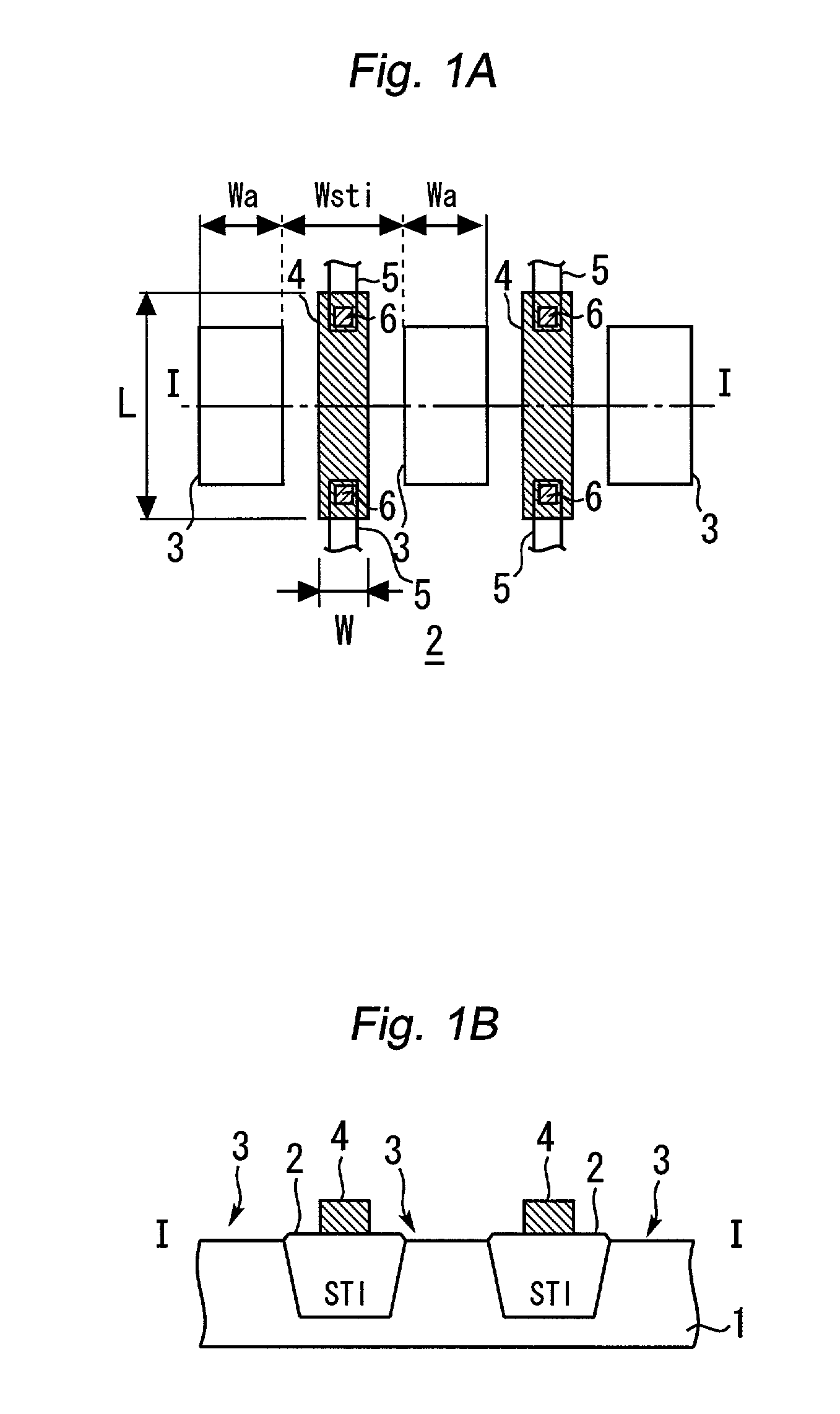
[0035]FIGS. 1A and 1B are schematic views of a semiconductor device practiced as the first embodiment of this invention. FIG. 1A is a plan view showing the first embodiment from above, and FIG. 1B is a schematic cross-sectional view taken on a dashed line I—I in FIG. 1A.
[0036]How the semiconductor device of the first embodiment is structured will now be described by referring to FIGS. 1A and 1B. This semiconductor device is manufactured by first forming an element isolating oxide film 2 through the STI process on a surface area of a semiconductor substrate 1. Over the element isolating oxide film 2, rectangular resistor elements 4 having a width W each are formed by use of an MOS transistor gate layer. The resistor elements 4 are composed illustratively of a polycrystal silicon film constituting the gate layer. As shown in FIG. 1A, element active regions 3 are formed in a manner contiguous with each resistor element 4 crosswise on both sides. In this structure, the element isolating...
second embodiment
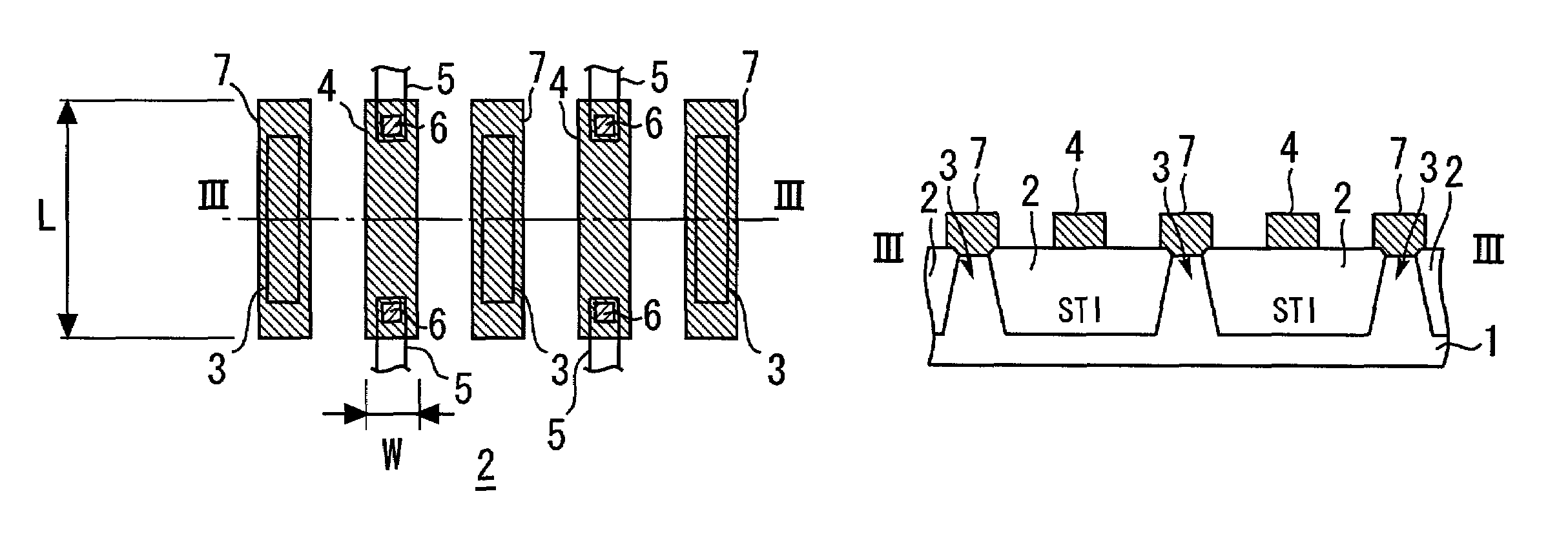
[0046]FIGS. 2A and 2B are schematic views of a semiconductor device practiced as the second embodiment of this invention. FIG. 2A is a plan view showing this semiconductor device of the second embodiment from above, and FIG. 2B is a schematic cross-sectional view taken on a dashed line II—II in FIG. 2A.
[0047]The semiconductor device of the second embodiment is structurally the same as that of the first embodiment in that the element active regions 3 flanking each resistor element 4 crosswise on both sides determine the width of the element isolating oxide film 2. The difference lies where the second embodiment has dummy gate electrodes 7 formed on the element active regions 3 on both sides of each resistor element 4, as shown in FIG. 2A. In describing the second and other embodiments of this invention below, their components having the same or corresponding functions as their counterparts in the first embodiment of FIGS. 1A through 1C are designated by like reference numerals, and t...
third embodiment
[0069]FIG. 10 is a schematic plan view of a semiconductor device practiced as the third embodiment of this invention, showing a horizontal structure of the device. The semiconductor device of FIG. 10 has diffusion layers 10 formed to function as resistor elements through implantation of impurities into the element active regions 3 of the semiconductor device in FIG. 1. Both ends of each diffusion layer 10 are connected via a contact layer 12 to an upper wiring layer 11.
[0070]In the semiconductor device of the third embodiment, as in the first embodiment, an element isolating oxide film 2 with resistor elements 4 formed thereon is divided into strips by the element active regions 3. This ensures planarization of the surface of the element isolating oxide film 2 during polishing by CMP. Forming the diffusion layers 10 in the element active regions 3 makes it possible to produce resistor portions of the diffusion layers 10 (i.e., diffusion layer resistor elements) contiguous with the r...
PUM
 Abstract
Description
Claims
Application Information