Optoelectronic transmission module and fabrication method thereof

a transmission module and optoelectronic technology, applied in the direction of optical elements, instruments, optical waveguide light guides, etc., can solve the problems of time-consuming replacement of defective elements, limited transmission speed and wideband communication of conventional circuit boards, and inability to perform optical coupling alignment between waveguide films

Active Publication Date: 2006-05-16
IND TECH RES INST
View PDF1 Cites 21 Cited by
  • Summary
  • Abstract
  • Description
  • Claims
  • Application Information

AI Technical Summary

Benefits of technology

[0006]It is therefore an object of the present invention to provide an optoelectronic transmission module capable of transmitting light signals and electrical signals at the same time without requiring a waveguide film or a fiber ribbon to be disposed in a substrate.
[0007]Another object of the present invention is to provide an optoelectronic transmission module capable of transmitting light signals and electrical signals at the same time and simple optical coupling between light transducers and a waveguide film or fiber ribbon without requiring a lens and prisms.

Problems solved by technology

Due to the physical characteristics of electrical interconnections, the transmission speed and wideband communication of conventional circuit boards is limited.
It is difficulty, however, to perform optical coupling alignment between the waveguide film and the light transducers because they are disposed in the substrate.
Hence, replacing the defective elements is time-consuming.
Hence, the optical coupling alignment is still difficult.

Method used


Image

  • Optoelectronic transmission module and fabrication method thereof
  • Optoelectronic transmission module and fabrication method thereof
  • Optoelectronic transmission module and fabrication method thereof

Examples


Embodiment Construction

[0013]The present invention provides a fabrication method for an optoelectronic transmissive module, as shown in FIGS. 1a to 1e.

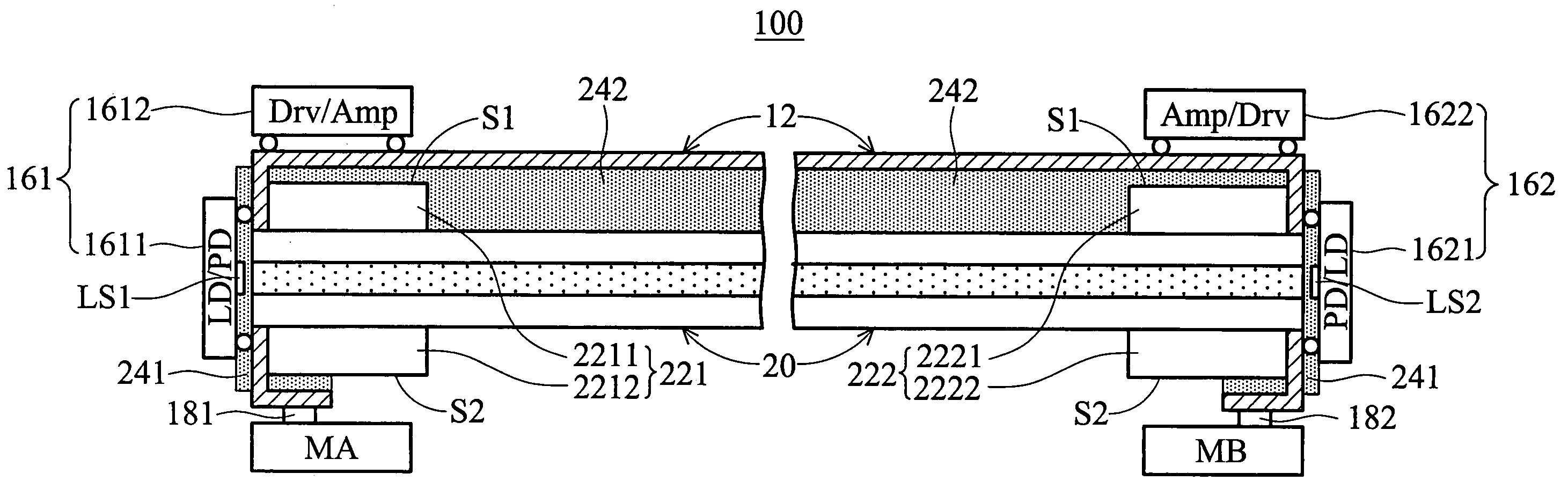
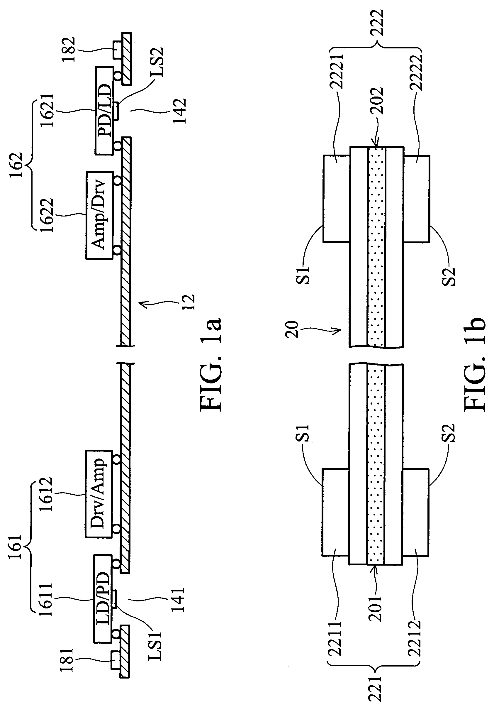
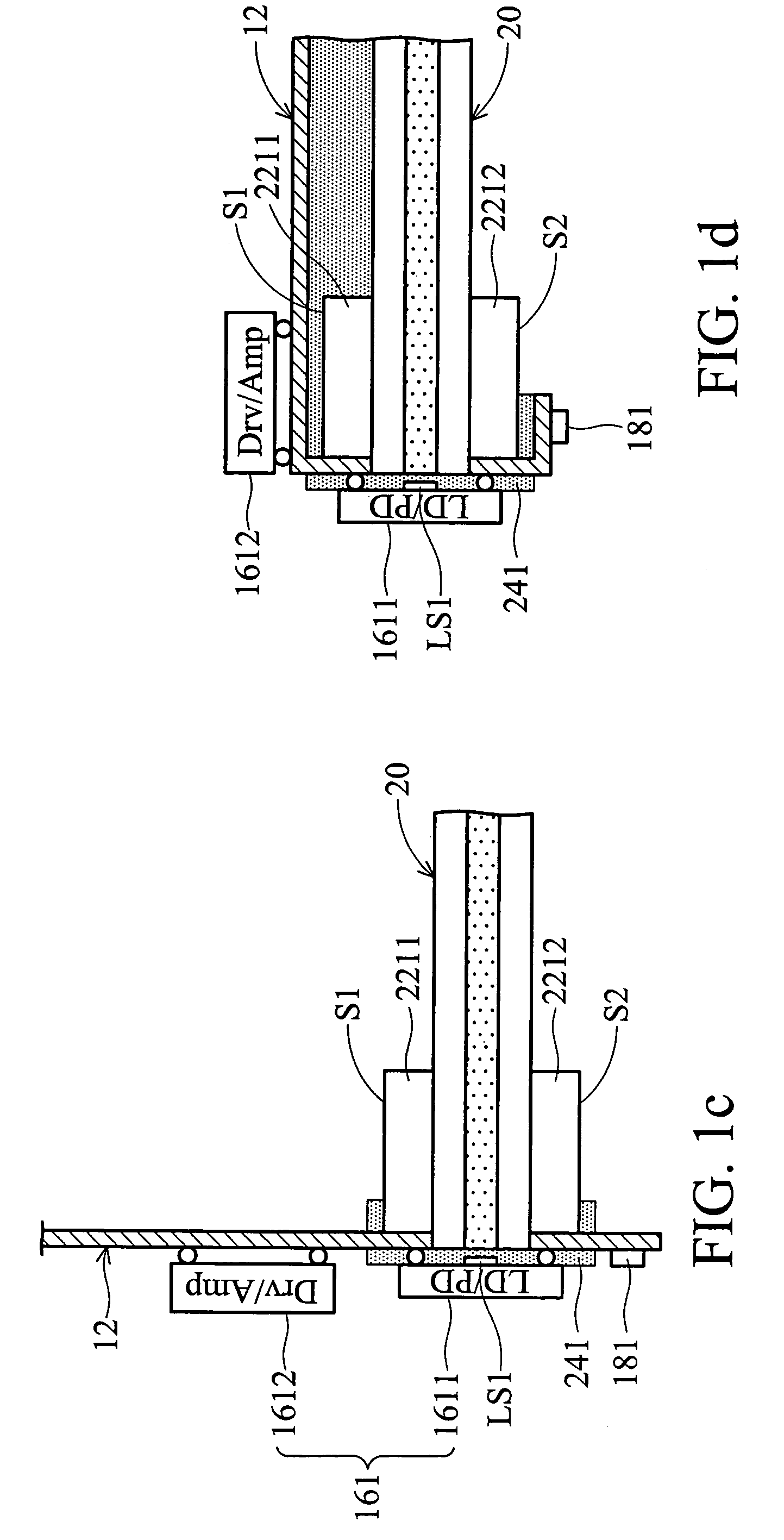
[0014]As shown in FIG. 1a, a circuit board 12 has two openings 141 and 142 on each side, the circuit board can be a flexible printed circuit board.

[0015]Next, first and second light transducers 161 and 162 are disposed on the circuit board 12, and aligned with the openings 141 and 142 of the circuit board 12 respectively. The first light transducer 161 has a light transmitter / detector LS1 aligned with the corresponding opening 141 of the circuit board 12. The second light transducer 162 has a light transmitter / detector LS2 aligned with the corresponding opening 142 of the circuit board 12. For example, the light transmission unit in 1611 of the light transducers 161 and the light detection unit in 1621 of the light transducers 162 constitute a light transmission / reception combination. The light transducer 161 has a light transmission / detection unit 1611 an...


PUM


Abstract

An optoelectronic transmission module. In the optoelectronic transmission module, a light transmissive element has first and second ends and top and bottom surfaces, a circuit board transmits electrical signals and has first and second openings. The circuit board is conformably extended from the top surface of the light transmissive element to the bottom surface such that the first and second openings are aligned with the first and second ends respectively. Two light transducers, each having a light transmitter / detector optically aligned with one of the first and second ends of the light transmissive element, wherein the light transducers transmit / receive light signals through the light transmissive element and the light transmitter / detector thereof. Two electrical interconnections are disposed on the circuit board and neighbored with the two ends of the light transmissive element respectively to interconnect the electrical signals.

Description

BACKGROUND OF THE INVENTION[0001]1. Field of the Invention[0002]The present invention relates to optoelectronic devices, and more particularly, to an optoelectronic transmission module and fabrication method thereof.[0003]2. Description of the Related Art[0004]Due to the physical characteristics of electrical interconnections, the transmission speed and wideband communication of conventional circuit boards is limited. Thus, a waveguide film and light transducers are combined to form an optoelectronic substrate to meet transmission requirements for high speed data communication. Because light transmission speed is much faster than electrical transmission speed, high transmission speed over a short-distance can be obtained.[0005]In conventional methods, substrates must be etched in order to install a waveguide film or light transducers for transmitting light signals on the same circuit board. It is difficulty, however, to perform optical coupling alignment between the waveguide film a...

Claims


Application Information

Patent Timeline
Patent Type & Authority Patents(United States)
IPC IPC(8): G02B6/12G02B6/36H04B10/00G02B6/42
CPCG02B6/4212
Inventor SHEN, LI-CHENG
Owner IND TECH RES INST
Why Eureka
Try Eureka