Semiconductor laser drive circuit

a laser drive circuit and semiconductor technology, applied in the direction of digital signal error detection/correction, instruments, recording signal processing, etc., can solve the problems of reducing the c/n ratio of a read signal, generating scoop noise and mode hopping noise, and affecting the response speed, etc., to achieve short emission time, reduce the number of wires, and high transfer rate

Inactive Publication Date: 2006-05-23
SONY CORP
View PDF8 Cites 0 Cited by
  • Summary
  • Abstract
  • Description
  • Claims
  • Application Information

AI Technical Summary

Benefits of technology

[0012]Accordingly, the number of wires is reduced, and the problem of out-of-timing pulses due to differences in wire length is solved. Light is thus emitted with a shorter emission time at a high transfer rate.

Problems solved by technology

As a result, this feedback light and the irradiating light interfere with each other to generate scoop noise and mode hopping noise.
This causes degradation of the C / N ratio of a read signal.
As a result, the response speed tends to become slower.
This problem is very difficult to alleviate.
Therefore, the semiconductor laser drive circuit has large power consumption and is disadvantageous in terms of heat dissipation.

Method used


Image

  • Semiconductor laser drive circuit
  • Semiconductor laser drive circuit
  • Semiconductor laser drive circuit

Examples


Embodiment Construction

[0019]With reference to the drawings, embodiments of the present invention will now be described.

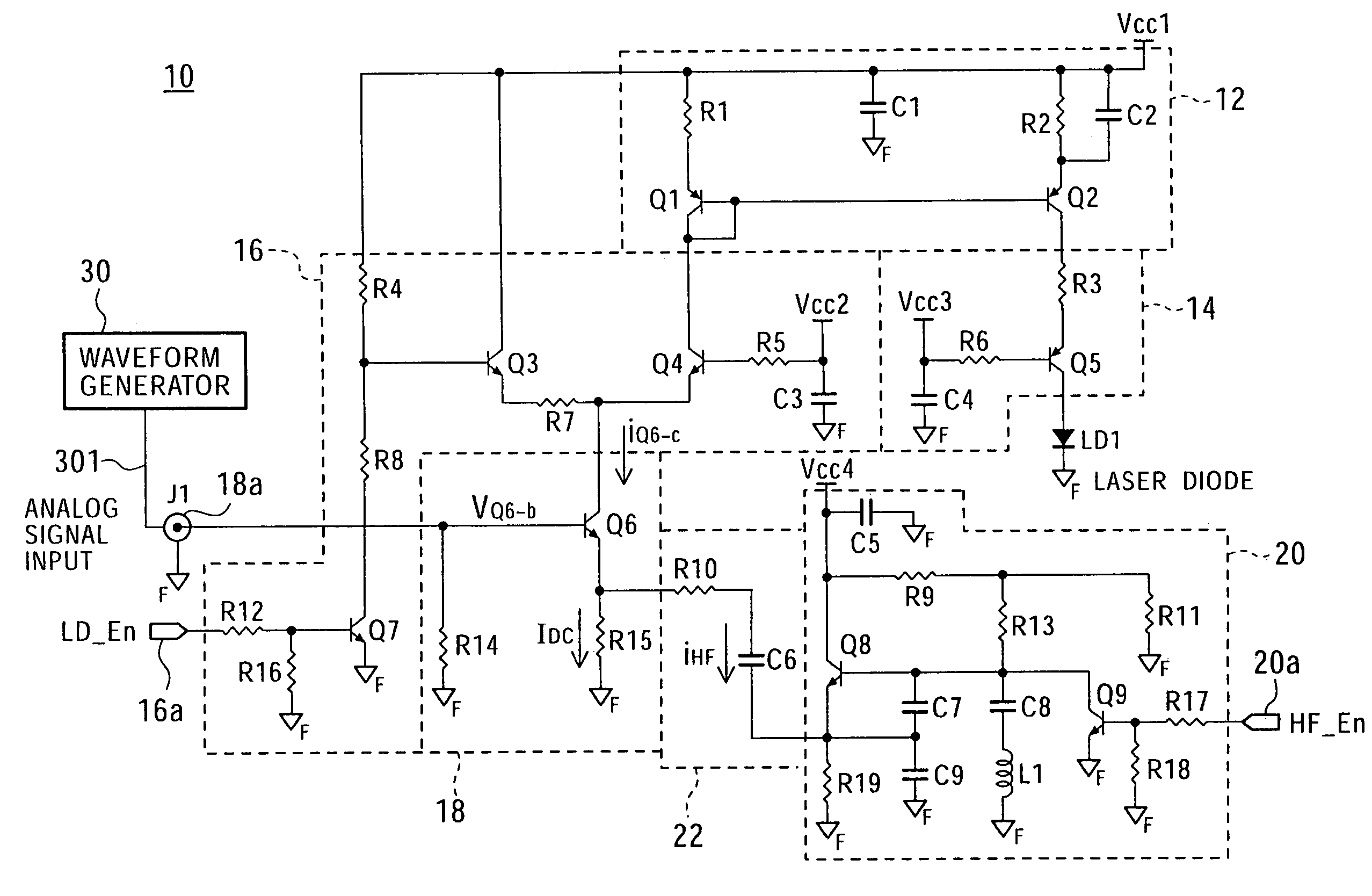
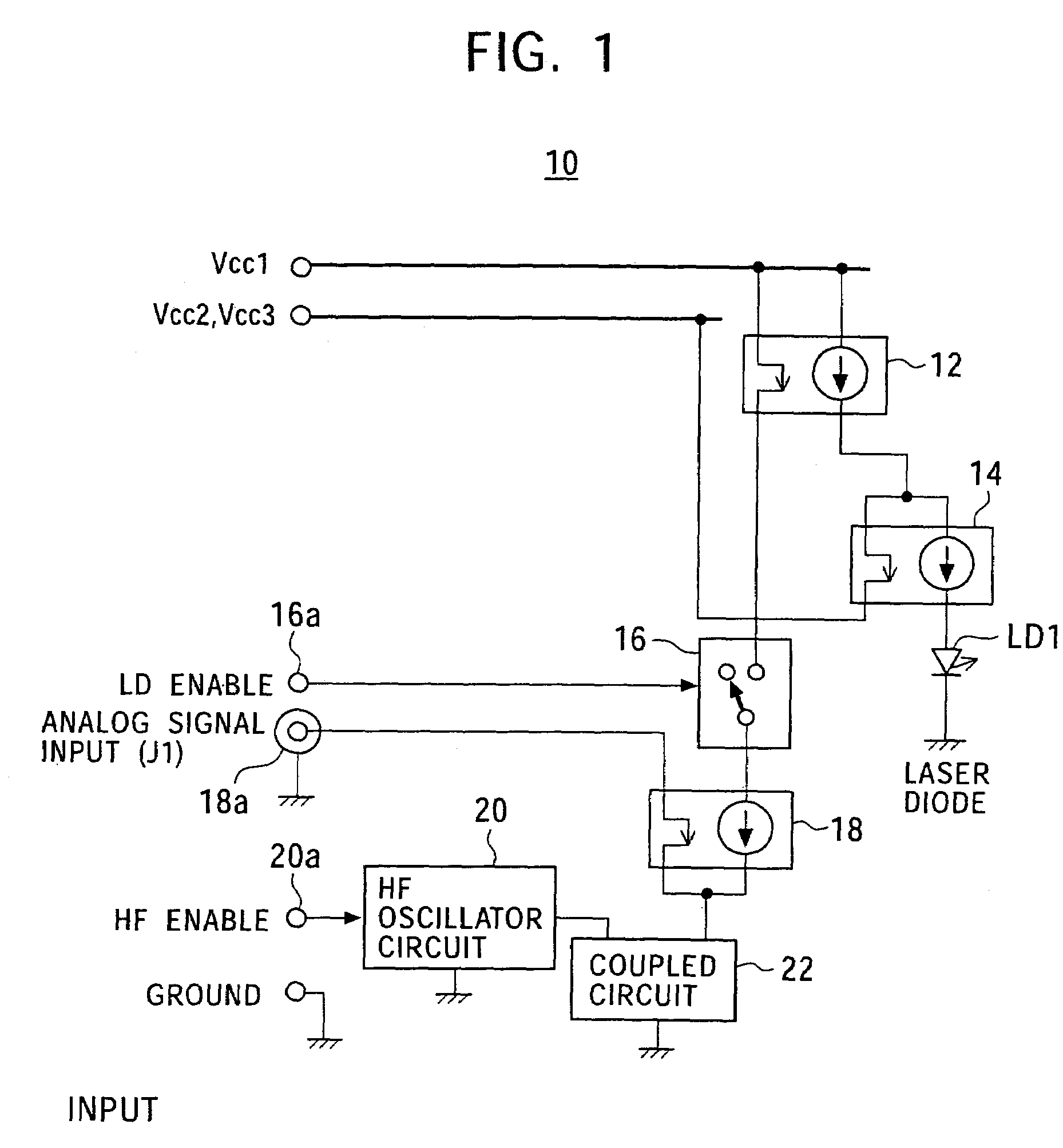
[0020]FIG. 1 is a block diagram showing the configuration of a laser driver for one laser in a semiconductor laser drive circuit of the present invention. FIG. 2 is a circuit diagram showing an example of the circuit configuration of the laser driver shown in FIG. 1.

[0021]Referring to FIGS. 1 and 2, a semiconductor laser drive circuit 10 includes a current mirror circuit 12, a common base circuit 14, a current switch circuit 16, a common emitter circuit (voltage-to-current converter circuit) 18, and a high frequency (HF) oscillator circuit 20.

[0022]The current mirror circuit 12 is used to supply current to a laser diode LD1 to cause the laser diode LD1 to emit light when a write mode and an erase mode are selected. The current mirror circuit 12 includes base-coupled PNP transistors Q1 and Q2, resistors R1 and R2, and a capacitor C2. The emitters of the transistors Q1 and Q2 are connected...


PUM

PropertyMeasurementUnit
cathode voltageaaaaaaaaaa
voltageaaaaaaaaaa
voltage dropaaaaaaaaaa

Abstract

A semiconductor laser drive circuit of the present invention reduces the number of wires, solves the out-of-timing problem of pulses due to differences in wire length, and emit short light pulses at a high transfer rate. A common emitter circuit (18) converts a voltage signal (J1) input at an input port (18a) into a current signal and, when reading information, adds the current signal to a signal output from a high-frequency oscillator circuit (20). High frequency components of the current signal converted from the voltage signal (J1) within a bandwidth of a transistor (Q6) are boosted. Degradation of the output signal of the high-frequency oscillator circuit (20) is kept at a minimum by a common base circuit including the transistor (Q6). A current switch circuit (16) cuts off or lets through the output current of a current mirror circuit (12).

Description

TECHNICAL FIELD[0001]The present invention relates to semiconductor laser drive circuits incorporated and used in optical disk drives for writing, erasing, and reading information from optical disks by irradiating the optical disks with laser light.BACKGROUND ART[0002]Semiconductor lasers in optical disk drives are used to read information from optical disks and, in the case of rewritable optical disks including phase-change optical disks, known as CD-RW, to write information to such optical disks.[0003]The output level of laser light of such semiconductor lasers is switched depending on whether to write, read, or erase information on optical disks. For example, when reading information, a semiconductor laser irradiates an optical disk with laser light at an output level lower than that when writing information. The semiconductor laser thus reads information without destructing a written pit on the optical disk.[0004]Laser light used to irradiate an optical disk to read information ...

Claims


Application Information

Patent Timeline
Patent Type & Authority Patents(United States)
IPC IPC(8): G11B7/00G11B7/006G11B7/126H01S5/042
CPCG11B7/0062H01S5/042G11B7/126
Inventor TANASE, HIRONOBU
Owner SONY CORP
Why Eureka
Try Eureka