Methods and circuitry for reducing intermodulation in integrated transceivers

a technology of integrated transceivers and intermodulation, applied in the field of high-speed telecommunications, can solve problems such as degrad achieve the effects of optimizing the performance of integrated circuits, reducing adverse effects of intermodulation, and reducing intermodulation adverse effects

Inactive Publication Date: 2006-05-23
AVAGO TECH INT SALES PTE LTD
View PDF3 Cites 15 Cited by
  • Summary
  • Abstract
  • Description
  • Claims
  • Application Information

AI Technical Summary

Benefits of technology

[0005]Conventional integrated transceivers which include more than one voltage-controlled oscillator on the integrated circuit suffer from the problem that undesirable coupling through a variety of mechanisms causes intermodulation, thereby degrading the performance of the integrated circuit. The present invention provides methods and circuitry that reduce adverse impacts of intermodulation and optimize performance of integrated circuits that include two or more oscillator circuits on the same chip. In one embodiment, intermodulation is reduced in a transceiver device that includes a transmitter and a receiver on the same chip. The invention adjusts the relative power ratio of the receiver VCO and the transmitter VCO, or adjusts the relative loop bandwidths of the receiver and transmitter PLLs, or a combination of both to minimize intermodulation.
[0006]According to a specific embodiment of the invention, the injection lock frequency range of one VCO and its power when operating in a free running mode are first measured. Based on the injection lock frequency range and the free running power of the VCO, the invention then determines the amount of crosstalk power (or injection power). This information is used along with the loop bandwidth of each PLL to adjust the relative power and bandwidth ratios in the receiver and the transmitter to minimize intermodulation. This is achieved, according to a specific embodiment of the invention first locking a first PLL (transmitter or receiver) to a reference, while the second PLL is opened so that its VCO is free running. When the reference frequency of the first PLL is close enough to the free running VCO frequency of the second PLL (i.e., within the injection lock frequency range), the free running VCO will be injection locked to the first PLL due to the various crosstalk mechanisms. By measuring the injection lock frequency range Δωm, the amount of crosstalk signal power Pi can be determined by an equation that includes the free-run frequency ωo, the que (Q) of the loop filter (LC tank), and the free-run VCO power Po. When the second PLL is closed and locked to another reference which frequency is slightly different from the first one, intermodulation between the two phase-locked loops will occur. The modulation index is determined by both the PLL bandwidth and the free run VCO injection lock range, which mainly depends on the power ratio Pi / Po. By properly utilizing the trade off between PLL loop bandwidth and the VCO power ratio, the invention minimizes undesirable intermodulation.
[0007]Accordingly, in one embodiment, the present invention provides a method of reducing intermodulation between a first VCO in a first PLL and a second VCO in a second PLL, including: measuring an injection lock frequency range of the second VCO with respect to the first VCO; measuring a signal power of the second VCO; determining a crosstalk power between the first and the second VCOs using the measured injection lock frequency range and the measured signal power of the second VCO; and adjusting a signal power ratio between the first VCO and the second VCO to reduce intermodulation.

Problems solved by technology

Conventional integrated transceivers which include more than one voltage-controlled oscillator on the integrated circuit suffer from the problem that undesirable coupling through a variety of mechanisms causes intermodulation, thereby degrading the performance of the integrated circuit.

Method used


Image

  • Methods and circuitry for reducing intermodulation in integrated transceivers
  • Methods and circuitry for reducing intermodulation in integrated transceivers
  • Methods and circuitry for reducing intermodulation in integrated transceivers

Examples


Embodiment Construction

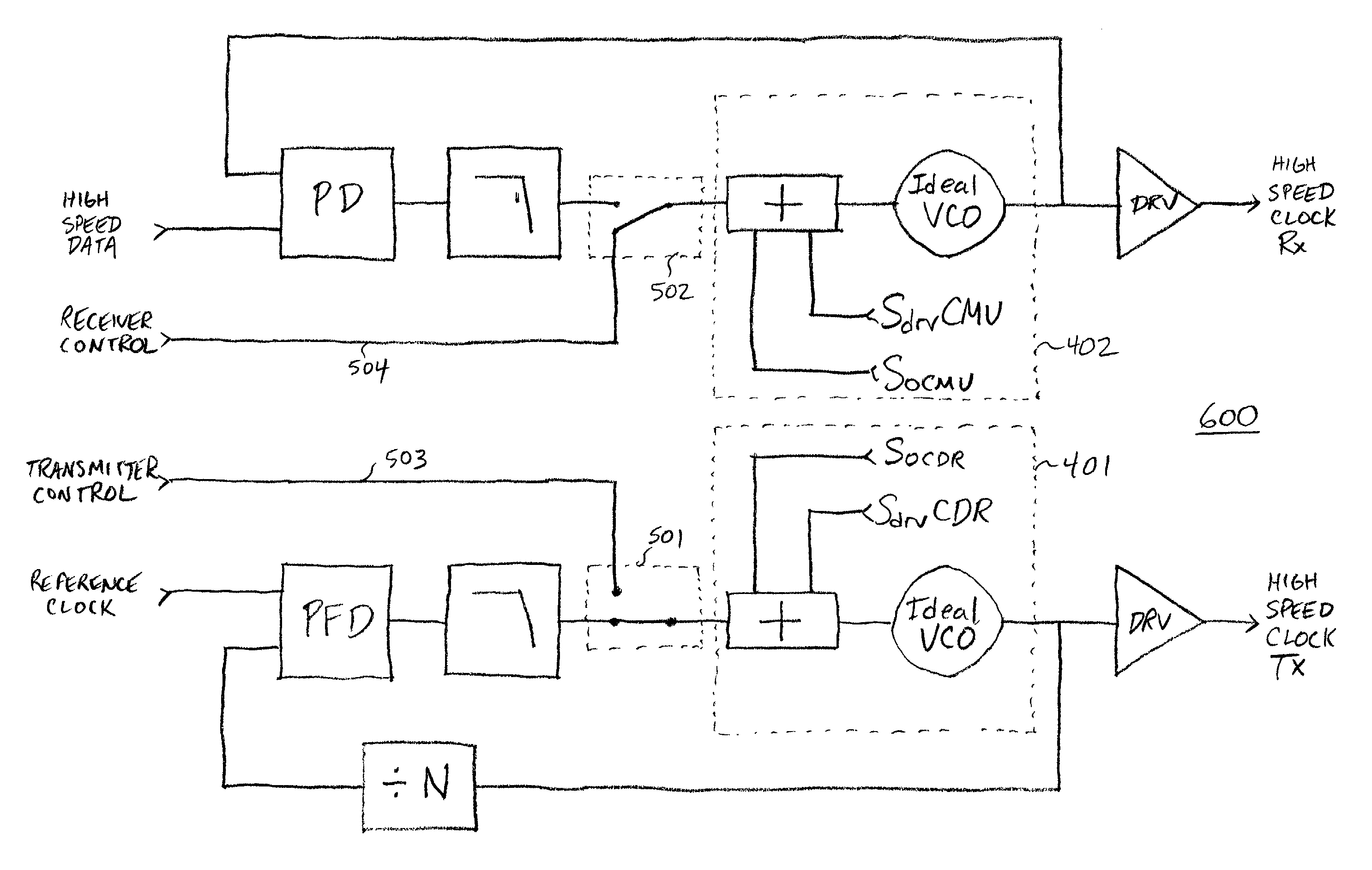
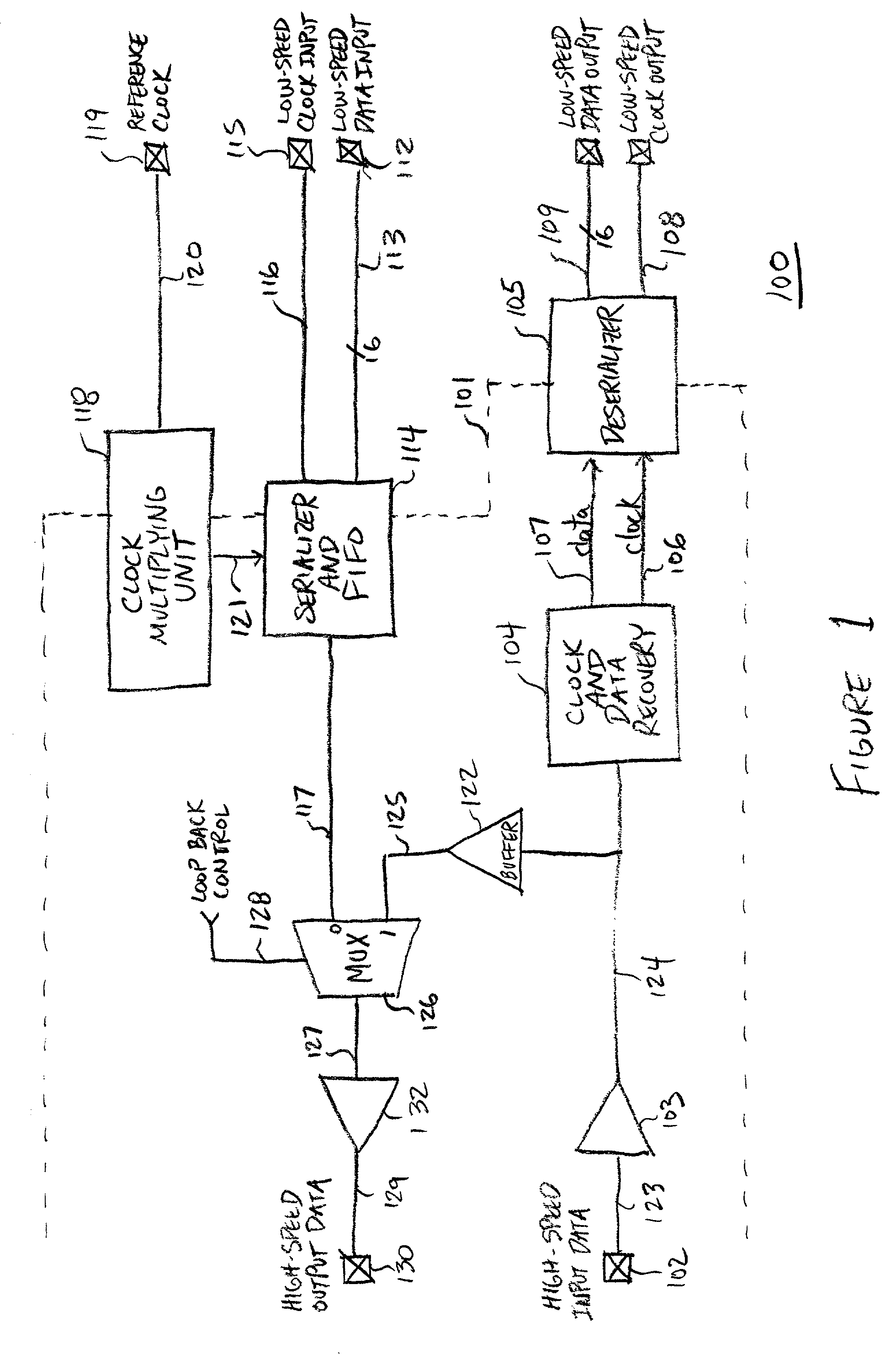
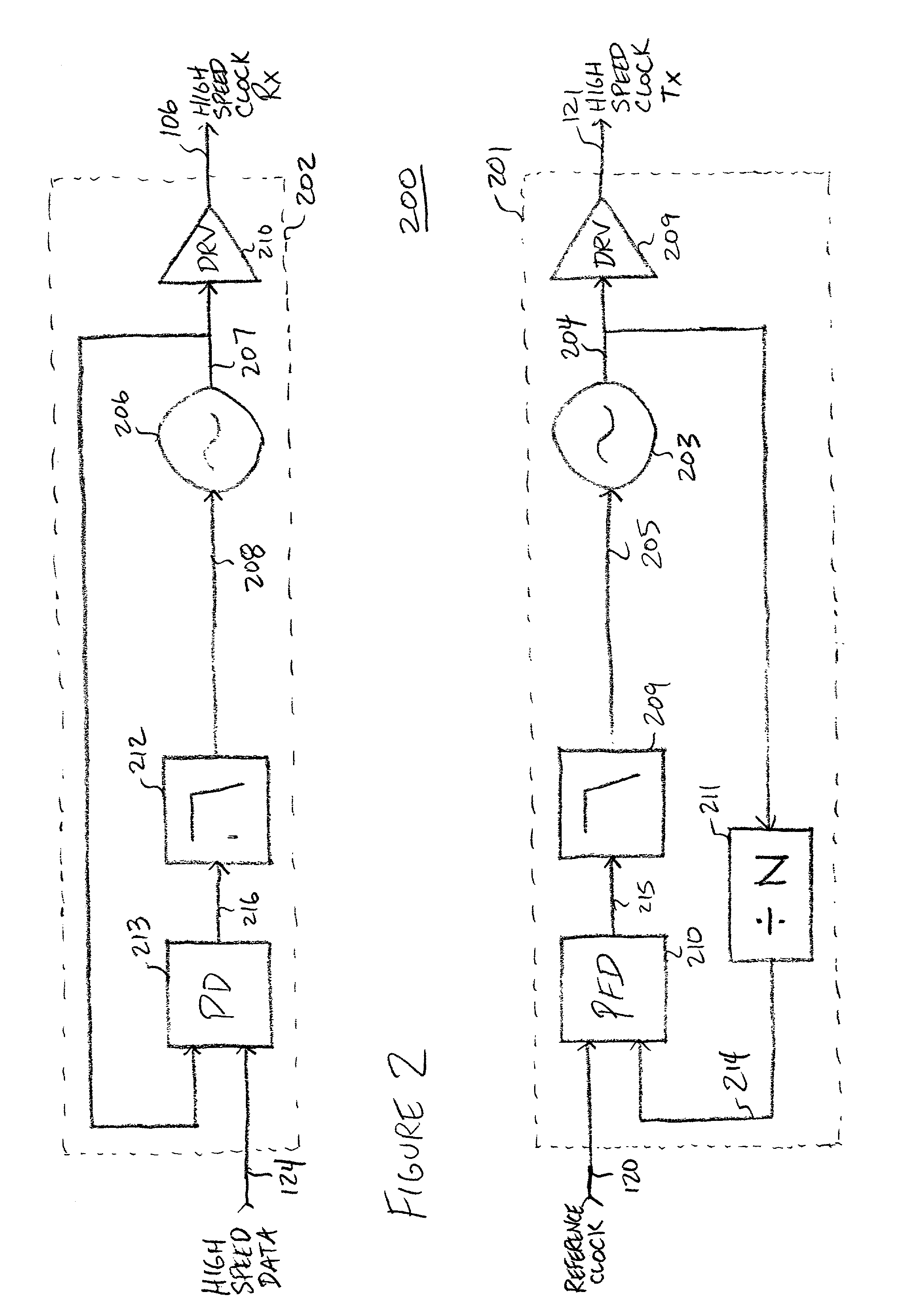
[0019]Since intermodulation through the various cross-talk mechanisms exists whenever two VCOs are fabricated on the same integrated circuit, regardless of the circuit context, the methods according to the present invention can be applied to any circuit configuration in which two VCOs are fabricated on the same die. For illustrative purposes only, the present invention is described in the context of an integrated communications transceiver that includes one VCO in the transmitter and another in the receiver. Specifically, the VCOs are part of phase-locked loops within a transmitter and receiver. In one exemplary embodiment described herein, the PLL having a VCO within the receiver is part of a clock and data recovery (CDR) unit, and the PLL having a VCO within the transmitter is part of the clock multiplying unit (CMU).

[0020]The transceiver includes a transmitter and a receiver. The receiver portion of the transceiver includes a clock and data recovery (CDR) unit which recovers the ...


PUM


Abstract

Methods and circuitry reduce adverse impacts of intermodulation and optimize performance of integrated circuits that include two or more oscillator circuits on the same chip. In one embodiment, intermodulation between voltage-controlled oscillators (VCOs)in the receiver and transmitter paths of a transceiver is reduced by adjusting relative power of the VCOs and / or bandwidths of the phase-locked loops (PLLs). The invention measures the injection lock frequency range of the VCOs based on which transmitter and receiver VCO power and loop bandwidths are adjusted.

Description

BACKGROUND OF THE INVENTION[0001]The present invention relates in general to the field of high-speed telecommunications, and in particular to integrated transceivers that include a voltage-controlled oscillator (VCO) in the transmitter and another VCO in the receiver portion of the transceiver.[0002]A single integrated circuit acting as a transceiver combines both a transmitter and a receiver on a single die. Such an integrated circuit has the advantages of reducing the communication system cost and providing easier diagnostic loop-back functions. A phase-locked loop (PLL) is an extremely useful system that is commonly used in a number of different applications and especially in communication systems. The heart of a PLL is a voltage-controlled oscillator (VCO) whose ideal output is a periodic signal the frequency of which is controlled by an input voltage.[0003]In the context of a transceiver, analog PLL technology has been used for both transmitter and receiver circuits due to its ...

Claims


Application Information

Patent Timeline
Patent Type & Authority Patents(United States)
IPC IPC(8): H04B1/10H03L1/00H03L7/07
CPCH03L1/00H04B1/109H03L7/07
Inventor CAI, YIJUN
Owner AVAGO TECH INT SALES PTE LTD
Why Eureka
Try Eureka