Semiconductor device and production method therefor

a technology of semiconductors and semiconductors, applied in the direction of multiple way valves, mechanical equipment, engine components, etc., can solve the problems of insufficient electrical connection, cumulative dimensional differences between the interconnection pattern and the bump electrode, and liable deformation of the interconnection pattern, so as to prevent the edge from touching

Active Publication Date: 2006-05-30
SHENZHEN TOREY MICROELECTRONIC TECH CO LTD
View PDF8 Cites 8 Cited by
  • Summary
  • Abstract
  • Description
  • Claims
  • Application Information

AI Technical Summary

Benefits of technology

[0028]Even if the interconnection pattern deforms due to the pressing of the semiconductor chip, the edge touch i

Problems solved by technology

In production of the COF device, the interconnection pattern is liable to deform when the semiconductor chip is mounted on the flexible wiring board by pressing the semiconductor chip against the flexible wiring board.
The expansion and contraction of the insulation tape significantly influence the positioning of the bump electrodes with respect to the interconnection pattern for the mounting, resulting in a cumulative dimensional difference between the interconnection pattern and the bump electrodes.
This makes it difficult to provide sufficient contact areas between the interconnection pattern and the bump electrodes, resulting in insufficient electrical connection.
In addition, the interconnection pattern having a reduced thickness is more liable to deform when the semiconductor chip is pressed against the flexible wiring board.
Therefore, the edge touch is more liable to occur.
Therefore, the semiconductor chip is liable to slide on the resin partly present between the electrodes of the semiconductor chip and the interconnection pattern when the semic

Method used


Image

  • Semiconductor device and production method therefor
  • Semiconductor device and production method therefor
  • Semiconductor device and production method therefor

Examples


second embodiment

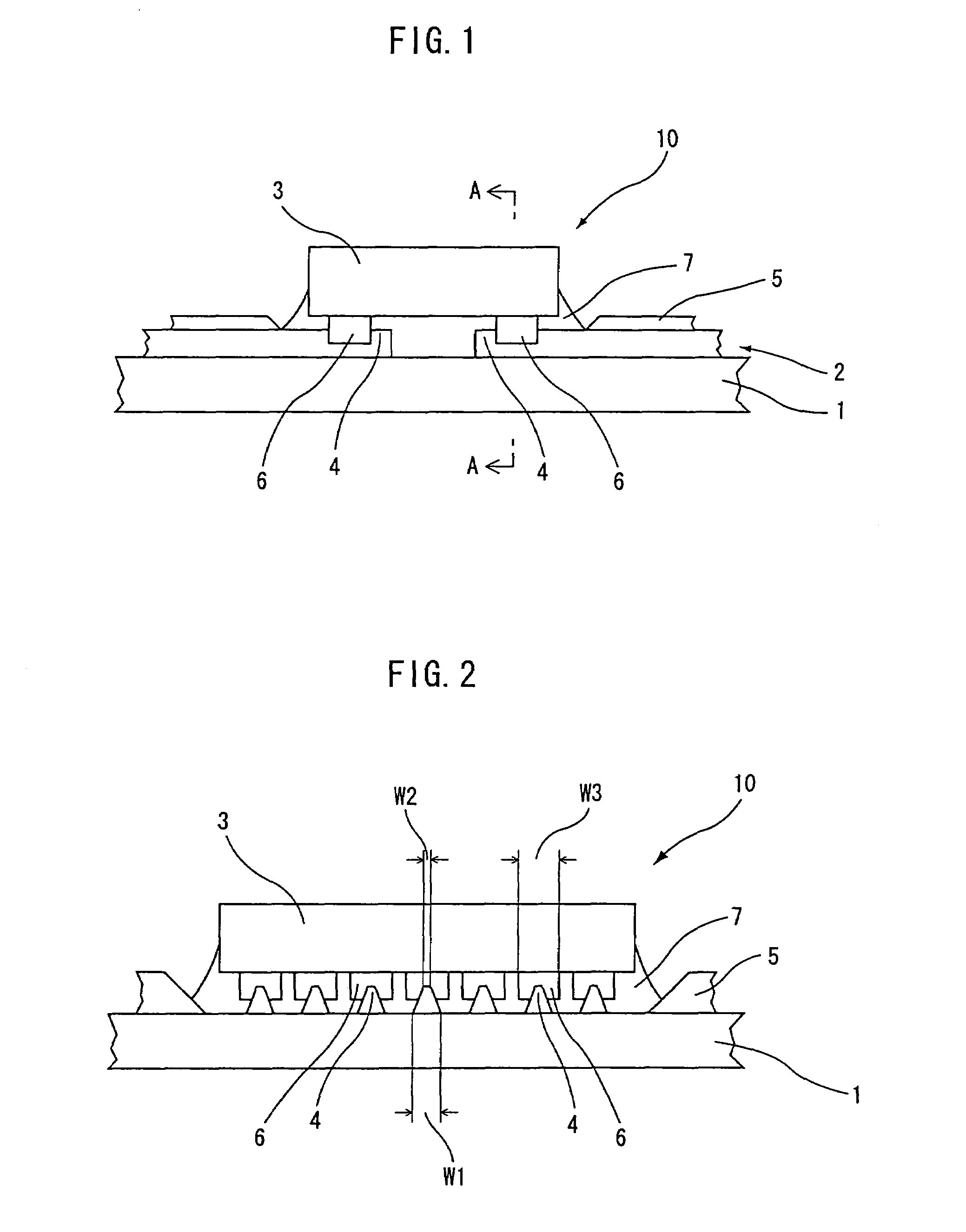
[0079]A semiconductor device production method according to a second embodiment is a modification of the semiconductor device production method according to the first embodiment. In this production method, the semiconductor device 10 (see FIGS. 1 and 2) is produced in substantially the same manner as in the production method according to the first embodiment, except that the semiconductor chip pressing and heating step is modified. Therefore, no explanation will be given to the step of positioning and mounting the semiconductor chip 3 on the resin 7 and the steps precedent thereto (see FIGS. 3(a) to 5(a) and FIGS. 3(b) to 5(b)), and only the step of pressing and heating the semiconductor chip 3 will be described with reference to FIGS. 8(a), 8(b), 9(a) and 9(b).

[0080]In the second embodiment, as shown in FIGS. 8(a) and 8(b), the semiconductor chip 3 is pressed against the film substrate 1 at a pressure of about 250×10−4 gf / μm2 and heated at about 230° C. to about 250° C. for about 1...

third embodiment

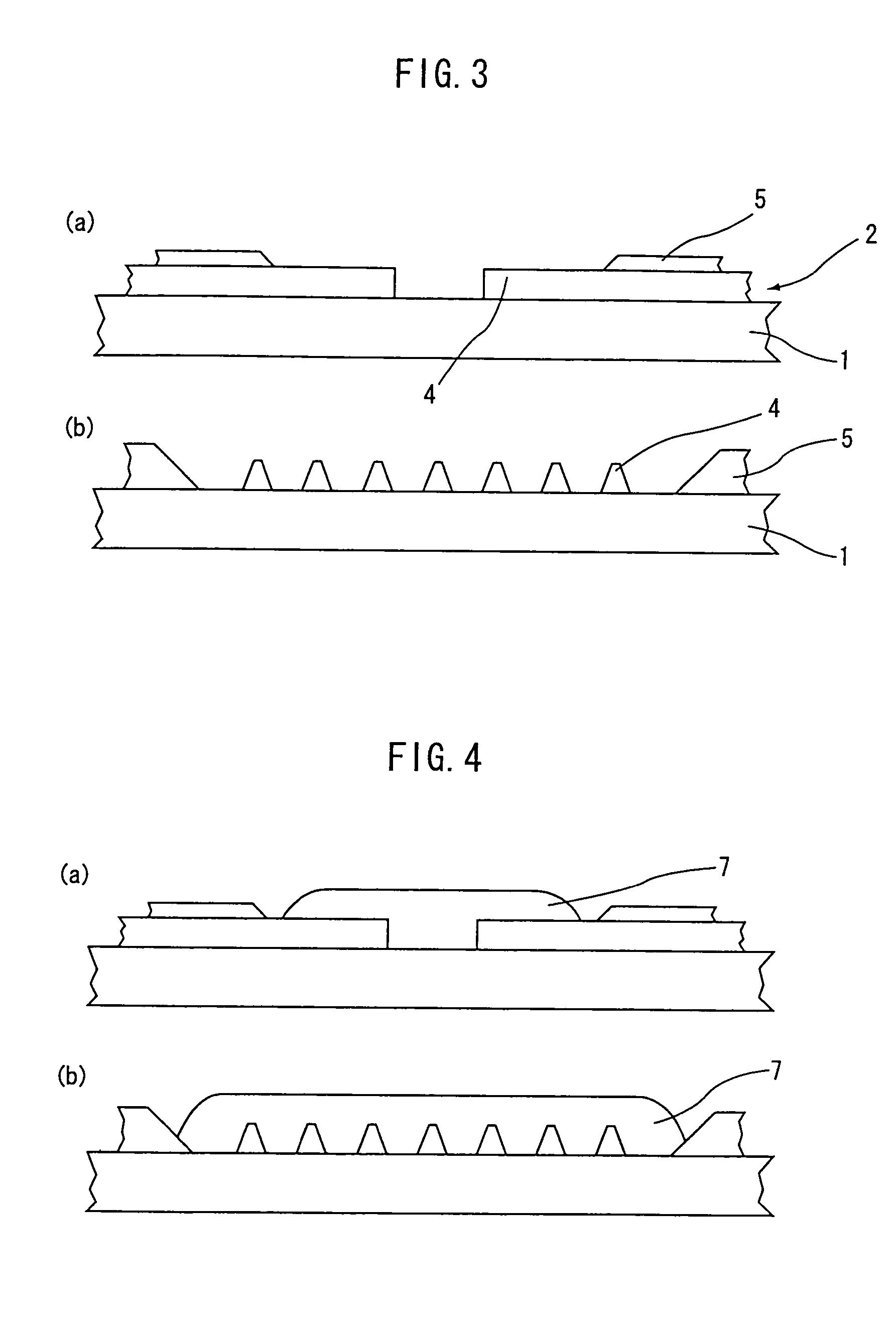
[0082]The construction of a COF semiconductor device according to a third embodiment of the present invention will be described with reference to FIG. 10. FIG. 10 is an enlarged partial view of the COF semiconductor device according to the third embodiment.

[0083]The COF semiconductor device according to the third embodiment has substantially the same construction as the semiconductor device 10 according to the first or second or embodiment (see FIGS. 1 and 2), except that alloy layers 38 of an alloy of metal materials for the projections 4 and the bump electrodes 6 are present in connection interfaces between the projections 4 of the interconnection pattern 2 and the bump electrodes 6 as shown in FIG. 10. Thus, the connection reliability is further improved.

[0084]A semiconductor device production method according to the third embodiment is substantially the same as the production method according to the first embodiment, except that the semiconductor chip pressing and heating step i...

fourth embodiment

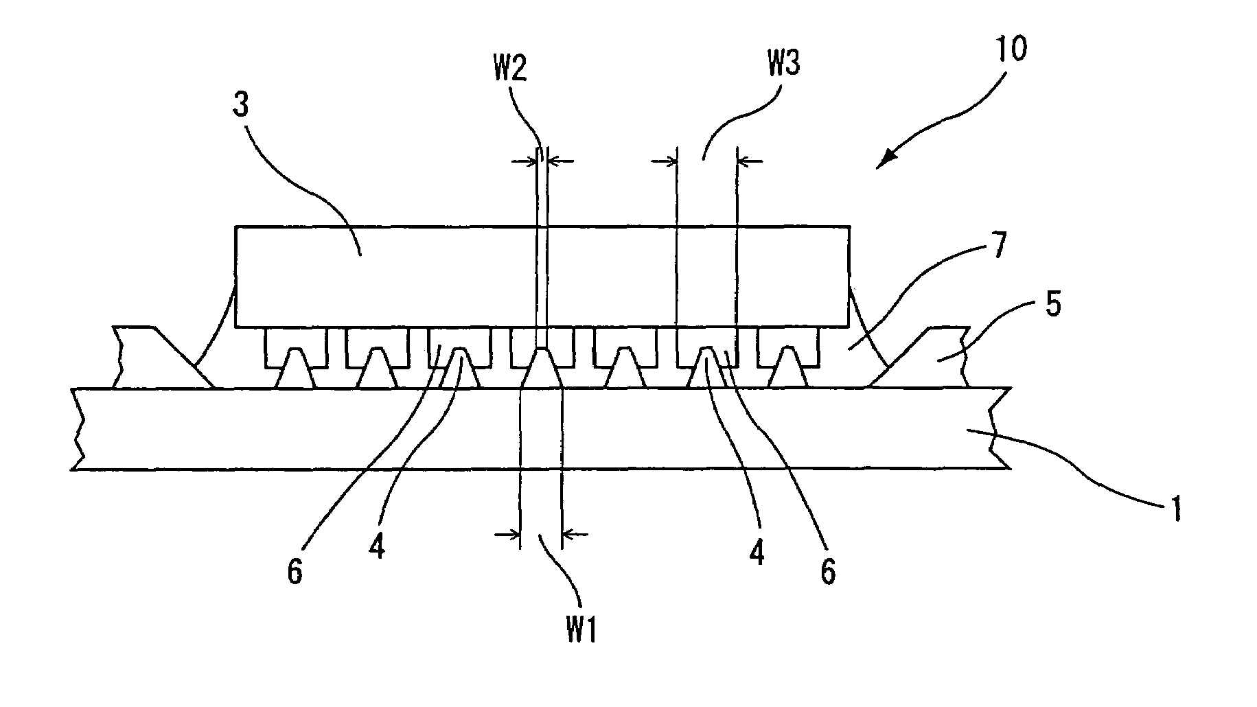
[0090]The construction of a COF semiconductor device according to a fourth embodiment of the present invention will be described with reference to FIGS. 14 and 15. FIG. 14 is a diagram schematically illustrating the construction of the COF semiconductor device according to the fourth embodiment, and FIG. 15 is a sectional view of the COF semiconductor device taken along a line B—B in FIG. 14.

[0091]As shown in FIGS. 14 and 15, the COF semiconductor device 40 according to the fourth embodiment has substantially the same construction as the semiconductor device 10 according to the first or second embodiment (see FIGS. 1 and 2), except that a resin portion 47 provided between the semiconductor chip 3 and the film substrate 1 contains conductive particles 49 dispersed therein. Some of the conductive particles 49 are present in the connection interfaces between the projections 4 of the interconnection pattern 2 and the bump electrodes 6, whereby the connection reliability is further impro...


PUM


Abstract

A semiconductor device includes a film substrate having an interconnection pattern provided on a surface thereof, a semiconductor chip mounted on the film substrate and having an electrode provided on a surface thereof, and an insulative resin portion provided between the film substrate and the semiconductor chip, the resin portion having been formed by applying an insulative resin on at least one of the film substrate and the semiconductor chip and filling a space defined between the film substrate and the semiconductor chip with the resin when the semiconductor chip is mounted on the film substrate, wherein the interconnection pattern has a projection which has a sectional shape tapered toward the electrode of the semiconductor chip and intrudes in the electrode thereby to be electrically connected to the electrode.

Description

CROSS-REFERENCE TO RELATED APPLICATIONS[0001]This application is related to Japanese patent application No. 2003-139023 filed on May 16, 2003, whose priority is claimed under 35 USC § 119, the disclosure of which is incorporated by reference in its entirety.BACKGROUND OF THE INVENTION[0002]1. Field of the Invention[0003]The present invention relates to a semiconductor device and a production method therefor. More specifically, the invention relates to a semiconductor device including a semiconductor chip bonded to and mounted on a flexible wiring board thereof, and a production method therefor.[0004]2. Description of the Related Art[0005]The following is known as the prior art of the present invention.[0006](1) A semiconductor device production method which comprises the steps of: stacking a semiconductor chip having Au bump electrodes at a predetermined position on a flexible wiring board; pressing the semiconductor chip against the flexible wiring board at a pressure of 0.1 to 0.3...

Claims


Application Information

Patent Timeline
IPC IPC(8): H01L21/48H01L29/40H01L21/60H01L23/498H01L23/50
CPCH01L23/49811H01L23/4985H01L24/16H01L24/29H01L24/32H01L24/81H01L24/83H01L24/90H01L2224/13099H01L2224/13144H01L2224/16225H01L2224/27013H01L2224/73204H01L2224/75252H01L2224/81203H01L2224/81801H01L2224/83051H01L2224/83192H01L2924/01004H01L2924/01005H01L2924/01013H01L2924/01029H01L2924/01033H01L2924/0105H01L2924/01078H01L2924/01079H01L2924/01082H01L2924/0781H01L2924/14H01L2224/1601H01L2224/81193H01L2224/2919H01L2224/32225H01L2924/01006H01L2924/014H01L2924/0665H01L2224/29101H01L2924/0132H01L2224/16238H01L2224/81191H01L2224/2929H01L2224/29111H01L2224/2939H01L2224/29355H01L2224/29444H01L2224/16501H01L2224/81825H01L2224/8183H01L2924/00H01L2924/00012H01L2924/00014F16K11/00F16K51/00
Inventor SEKO, TOSHIHARU
Owner SHENZHEN TOREY MICROELECTRONIC TECH CO LTD
Why Eureka
Try Eureka