
Radio frequency integrated circuit, and method for manufacturing the same

a radio frequency integrated circuit and integrated circuit technology, applied in the direction of transformer/inductance details, semiconductor devices, semiconductor/solid-state device details, etc., can solve the problem of limitative q value obtained by single-layer metal inductor, low quality factor of the inductor, and high parasitic capacitance and substrate loss, etc. problem, to achieve the effect of overcoming decoupling, reducing parasitic capacitance to the substrate, and increasing the thickness of the insulation layer

Active Publication Date: 2006-06-06
KEY FOUNDRY CO LTD
View PDF2 Cites 8 Cited by
  • Summary
  • Abstract
  • Description
  • Claims
  • Application Information

AI Technical Summary

Benefits of technology

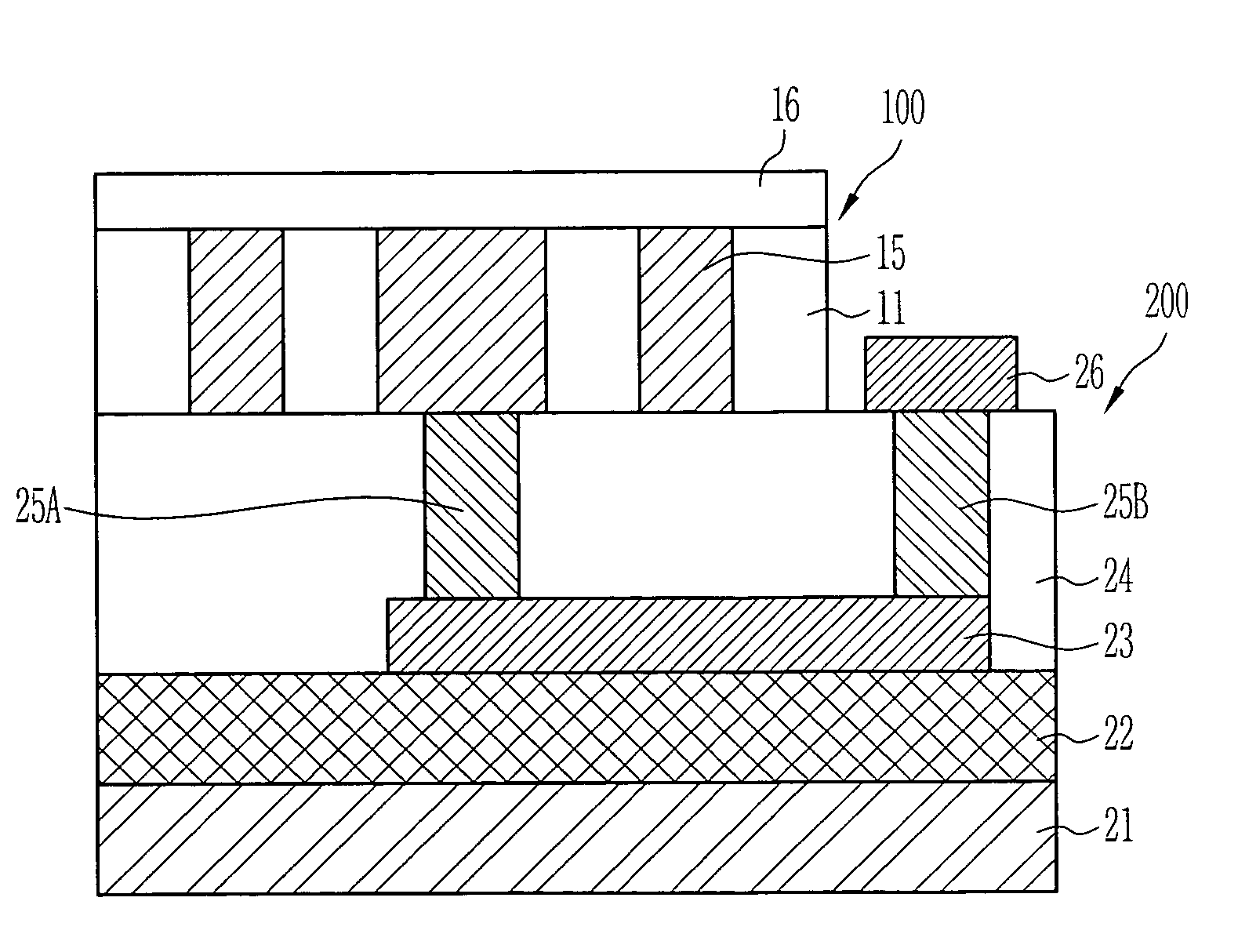
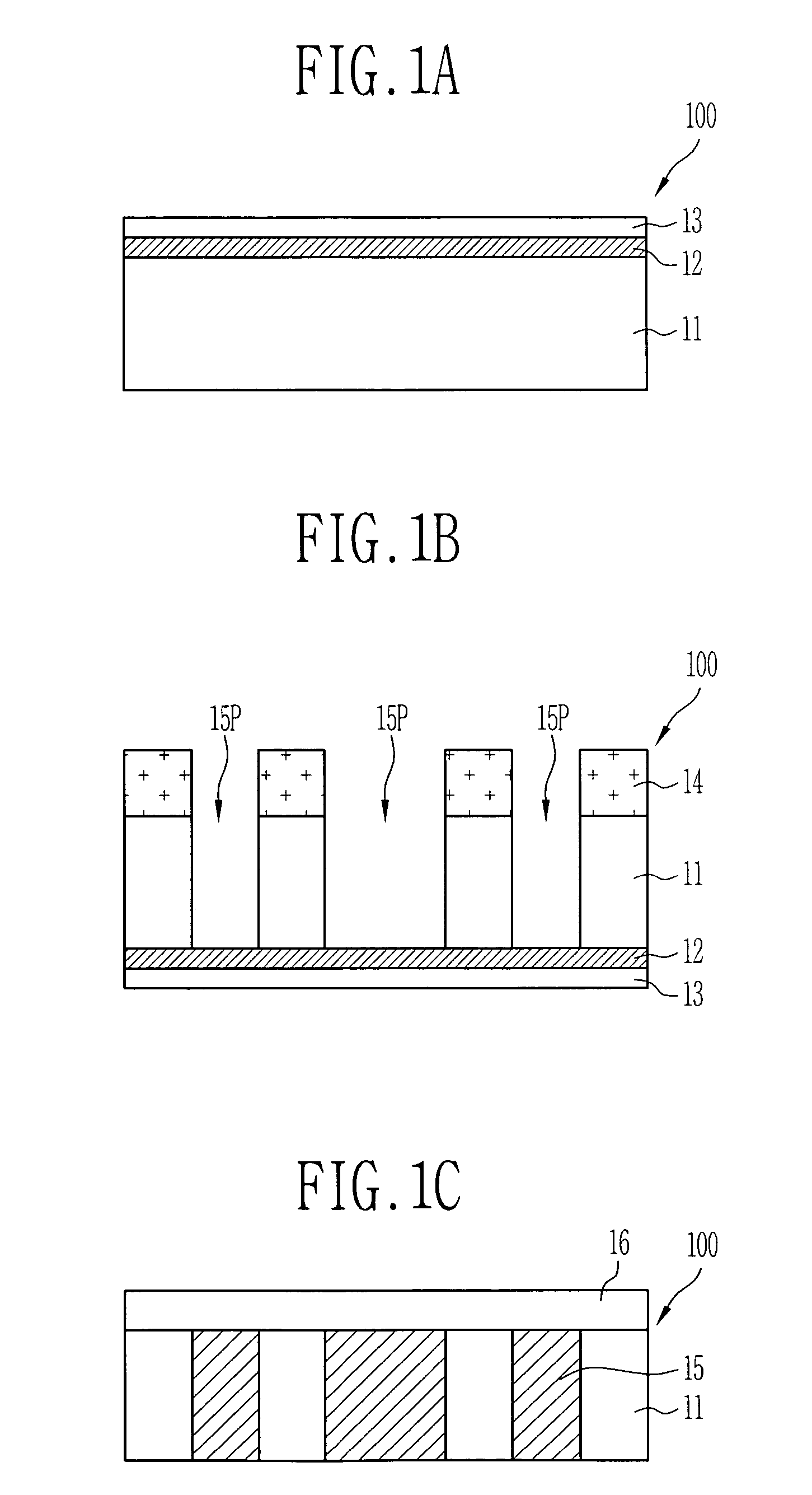
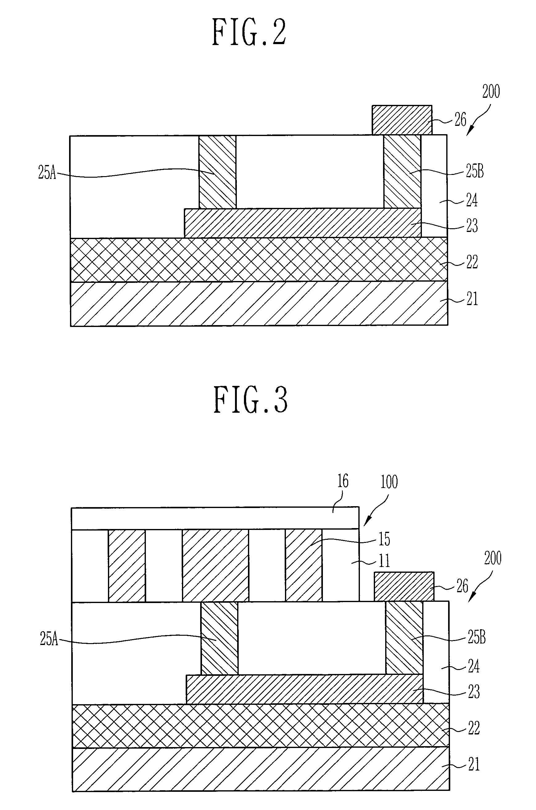
"The present invention provides a method for manufacturing a radio frequency integrated circuit that minimizes parasitic capacitance and decoupling. This is achieved by forming an inductor on a special substrate and bonding it onto another substrate with elements and wiring structures. The method includes steps of manufacturing the inductor substrate, forming an inductor coupling line on the element layer, adding an interlayer insulation layer with via contact plugs, and bonding the two substrates together. The invention also provides a radio frequency integrated circuit that includes a special substrate with an inductor and a passivation layer, and a method for manufacturing the same. The use of a special substrate and a chip scale integrated process allows for a more efficient and cost-effective manufacturing process."

Problems solved by technology

However, in both the RF-CMOS and the Bipolar / BiCMOS, the inductor has a low quality factor (hereinafter, referred as ‘Q’).
However, if a width of the metal lines excessively increases, the inductor area increases, which results in a high parasitic capacitance and substrate loss.
However, a Q value obtained by the single layer metal inductor is limitative.
In order to form a thicker metal inductor, a number of processes increases, and process failure occurs due to increase of entire height topology.
That is, it is difficult to form the thicker metal inductor on an on-chip.
However, the structure and properties of the inductor are deteriorated during a process for forming a uniform depth of inductor lines by double exposure or a process for forming a passivation layer after removing the photoresist layer.
A very complicated device having various functions is required for the future electronic system.
It implies a yield problem by integration of the multifunctional device, large expenses by complexity of the device, and technical limits.
In addition, wiring between sub systems has limits due to performance, muti-functions and reliability of the micro-electronic system.
Such factors are regarded as critical performance bottlenecks of the future IC generation.

Method used


Image

  • Radio frequency integrated circuit, and method for manufacturing the same
  • Radio frequency integrated circuit, and method for manufacturing the same
  • Radio frequency integrated circuit, and method for manufacturing the same

Examples


Embodiment Construction

[0033]A radio frequency integrated circuit and a method for manufacturing the same in accordance with a preferred embodiment of the present invention will now be described in detail with reference to the accompanying drawings.

[0034]In the case that it is described that one film is disposed ‘on’ another film or a semiconductor substrate, one film can directly contact another film or the semiconductor substrate, or the third film can be positioned between them. In the drawings, a thickness or size of each layer is exaggerated to provide clear and accurate explanations. Wherever possible, the same reference numerals will be used throughout the drawings and the description to refer to the same or like parts.

[0035]FIGS. 1A to 1C are cross-sectional diagrams illustrating sequential steps of a method for forming an inductor having a passivation layer on a first substrate to explain the method for manufacturing the radio frequency integrated circuit such as an RF-CMOS, Bipolar / SiGe and BiCM...


PUM


Abstract

The present invention discloses a radio frequency integrated circuit and a method for manufacturing the same. The radio frequency integrated circuit is manufactured by forming an inductor and a passivation layer on an insulator substrate of a first substrate, forming an element layer having a multi-layer wiring structure on a semiconductor substrate, an inductor coupling line formed on the top portion of the element layer, first and second via contact plugs formed on the inductor coupling line, and an input / output pad coupled to the second via contact plug on a second substrate, and bonding the first substrate onto the second substrate, so that the inductor of the first substrate can be coupled to the first via contact plug of the second substrate. As a result, the radio frequency integrated circuit includes the inductor having a high Q value, by forming the inductor sufficiently separately from the semiconductor substrate on which the elements have been formed.

Description

BACKGROUND[0001]1. Field of the Invention[0002]The present invention relates to a radio frequency integrated circuit, and a method for manufacturing the same, and more particularly to, a radio frequency integrated circuit which can minimize a parasitic capacitance by sufficiently increasing a distance between a semiconductor substrate on which elements have been formed and an inductor, and a method for manufacturing the same.[0003]2. Discussion of Related Art[0004]According to paradigm variations of information and communication fields, there are increasing demands for communications which can be performed irrespective of time and places. Wireless mobile communication fields have been rapidly developed, satisfying such demands. Radio frequency resources, and materials, devices and circuits operated at a radio frequency are required due to the development of the wireless communication. The radio frequency resources, materials, devices and circuits are used in a radio frequency domain...

Claims


Application Information

Patent Timeline
Patent Type & Authority Patents(United States)
IPC IPC(8): H01L21/8232H01L21/4763H01L27/04H01L23/522H01L25/065H01L27/06
CPCH01L25/0657H01L27/0611H01L23/5227H01L2225/06541H01L2924/0002H01L2924/00H01L27/04
Inventor PARK, SANG KYUNSHIN, CHAN SOO
Owner KEY FOUNDRY CO LTD
Learn More