Semiconductor optoelectronic device

a technology of optoelectronic devices and semiconductors, applied in semiconductor devices, lasers, semiconductor lasers, etc., can solve the problems of optical gain decline, optical confinement factor, optical cracks in nitride-based laser diodes, etc., to achieve the effect of increasing the optical confinement factor and improving durability and reliability

Active Publication Date: 2006-06-06
SAMSUNG ELECTRONICS CO LTD
View PDF7 Cites 46 Cited by
  • Summary
  • Abstract
  • Description
  • Claims
  • Application Information

AI Technical Summary

Benefits of technology

[0011]The present invention provides a semiconductor light emitting device having improved durability and reliability by effectively increasing an optical confinement factor.

Problems solved by technology

AlxGa1−xN has smaller lattice constant and thermal expansion coefficient than GaN used as a material of an n-type contact layer, which may cause cracks in a nitride-based laser diode.
Mode leakage reduces an optical confinement factor, and thus an optical gain decreases.
Therefore, the leakage mode increases the amount of current necessary to start oscillating a laser device and has a bad influence on a far-field pattern of the laser device.
A decrease in the optical confinement factor also increases the amount of current necessary to start oscillating the laser device, decreases an internal quantum efficiency, and also has a bad influence on the far-field pattern of the laser device.

Method used


Image

  • Semiconductor optoelectronic device
  • Semiconductor optoelectronic device
  • Semiconductor optoelectronic device

Examples


Embodiment Construction

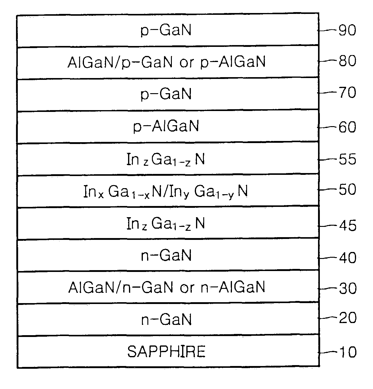
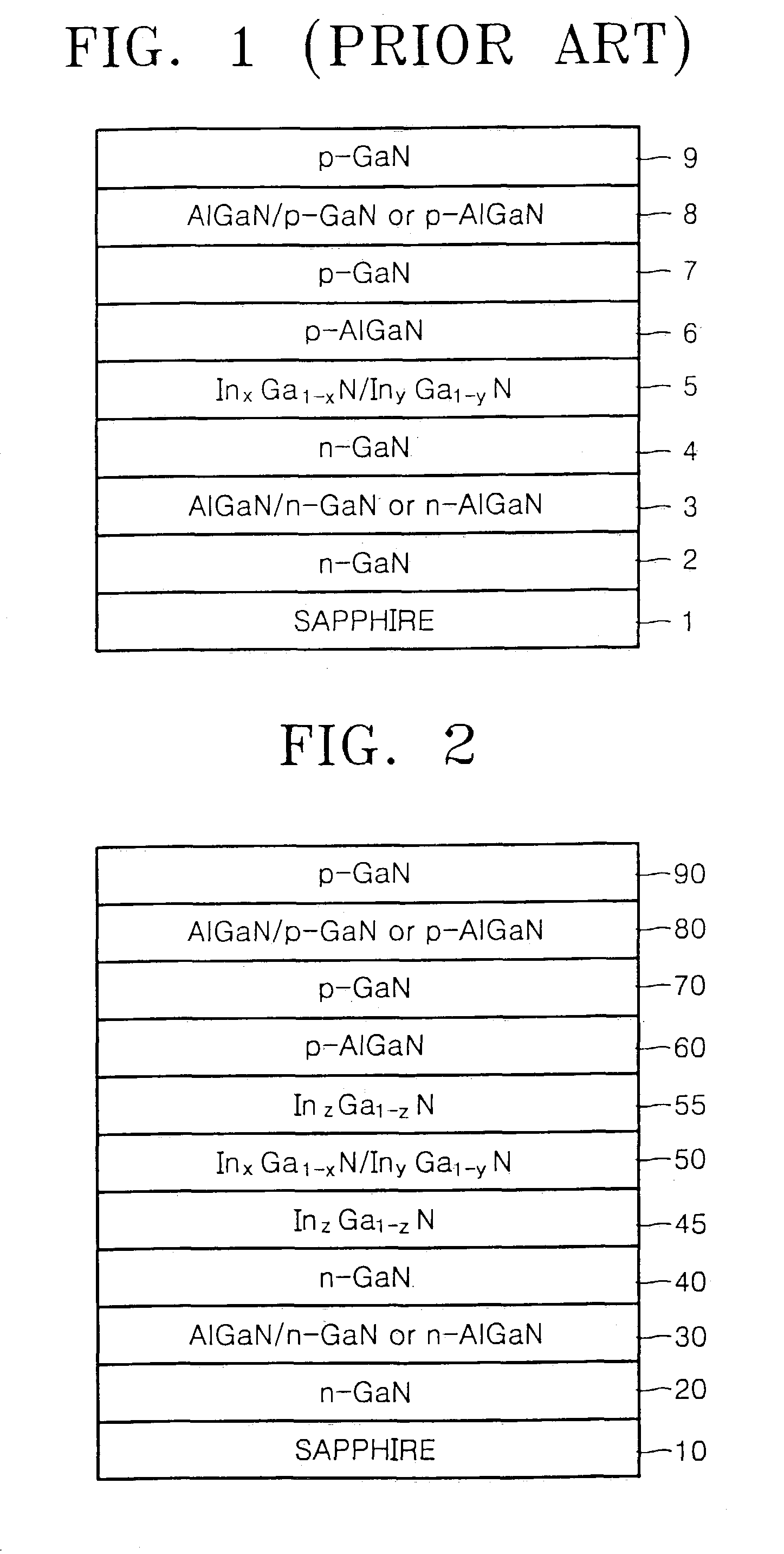
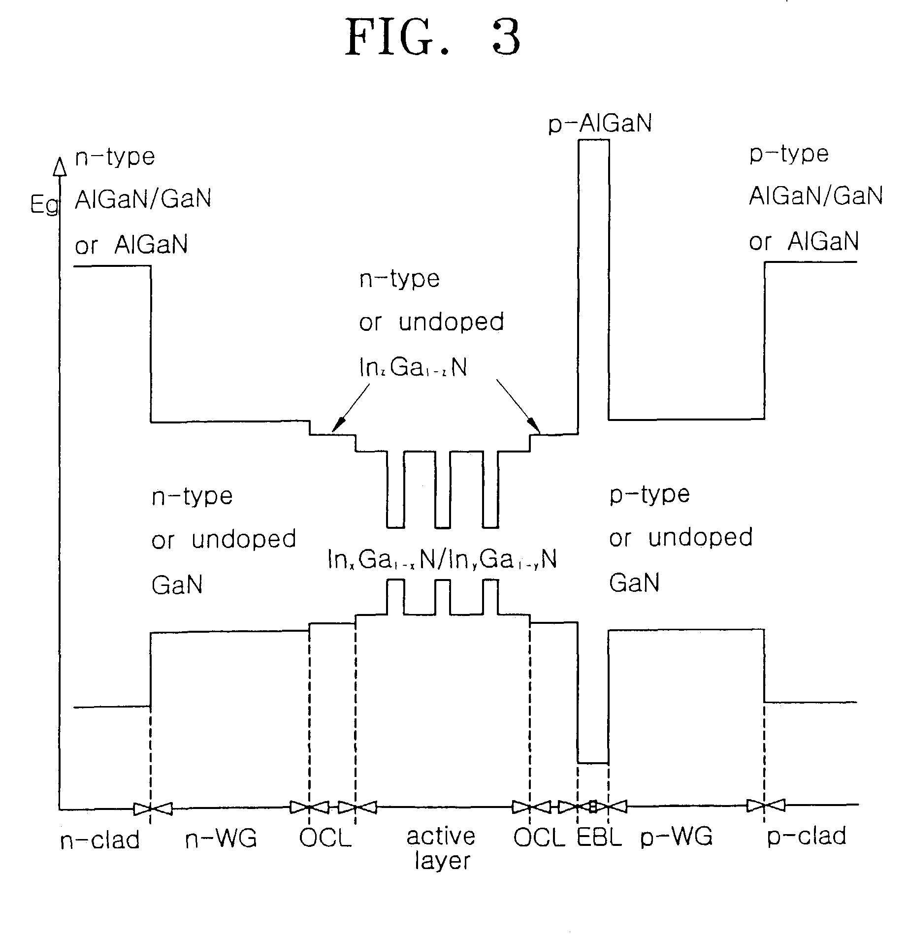
[0032]In order to increase an optical gain by increasing an optical confinement factor in a cladding layer having a maximum allowable aluminum composition ratio that does not cause any cracks, the present invention provides a semiconductor light emitting device having a light emitting device where an AlxInyGa1−x−yN (0≦x, y≦1, 0≦x+y≦1) optical confinement layer is interpolated between an active layer and an upper waveguide layer on the active layer and between the active layer and a lower waveguide layer under the active layer.

[0033]The semiconductor light emitting device according to the present invention has an enhanced internal quantum efficiency, and a reduced laser oscillation starting current and a reduced operation input power. The decrease in laser oscillation starting current and operation input power contributes to an extending life span of the semiconductor light-emitting device.

[0034]The semiconductor light-emitting device according to the present invention can be applied...


PUM


Abstract

A highly efficient semiconductor optoelectronic device is provided. The semiconductor optoelectronic device includes an active layer, an upper waveguide layer provided on the active layer and a lower waveguide layer provided under the active layer, an upper cladding layer provided on the upper waveguide layer and a lower cladding layer provided under the lower waveguide layer, a substrate supporting a deposited structure of the lower cladding layer, the lower waveguide layer, the active layer, the upper waveguide layer, and the upper cladding layer, and upper and lower optical confinement layers provided between the active layer and the upper waveguide layer and between the active layer and the lower waveguide layer, respectively, and having an energy gap that is smaller than those of the upper and lower waveguide layers but greater than that of the active layer.

Description

BACKGROUND OF THE INVENTION[0001]This application claims the priority of Korean Patent Application Nos. 2002-63539 and 2003-33842, filed on Oct. 17, 2002 and May 27, 2003, respectively, in the Korean Intellectual Property Office, the disclosure of which is incorporated herein in its entirety by reference.[0002]1. Field of the Invention[0003]The present invention relates to a semiconductor optoelectronic device, and more particularly, to a semiconductor optoelectronic device having a high optical efficiency.[0004]2. Description of the Related Art[0005]As shown in FIG. 1, a semiconductor laser device, which is one kind of nitride-based semiconductor optoelectronic device, has a sapphire substrate 1 as its base and includes an active layer 5 emitting or receiving light, n-type layers 2, 3, and 4 deposited on the sapphire substrate 1, and p-type layers 6, 7, and 8 deposited on the n-type layers 2, 3, and 4.[0006]In particular, the p-type layer 7 and the n-type layer respectively provide...

Claims


Application Information

Patent Timeline
Patent Type & Authority Patents(United States)
IPC IPC(8): H01S5/00H01S5/30H01S5/20H01S5/32H01S5/323H01S5/343
CPCB82Y20/00H01L33/02H01S5/20H01L33/32H01L33/06H01S5/34333H01S5/2009H01S5/3211
Inventor LEE, SUNG-NAMHA, KYOUNG-HOSAKONG, TAN
Owner SAMSUNG ELECTRONICS CO LTD
Why Eureka
Try Eureka