Method for fabricating memory device

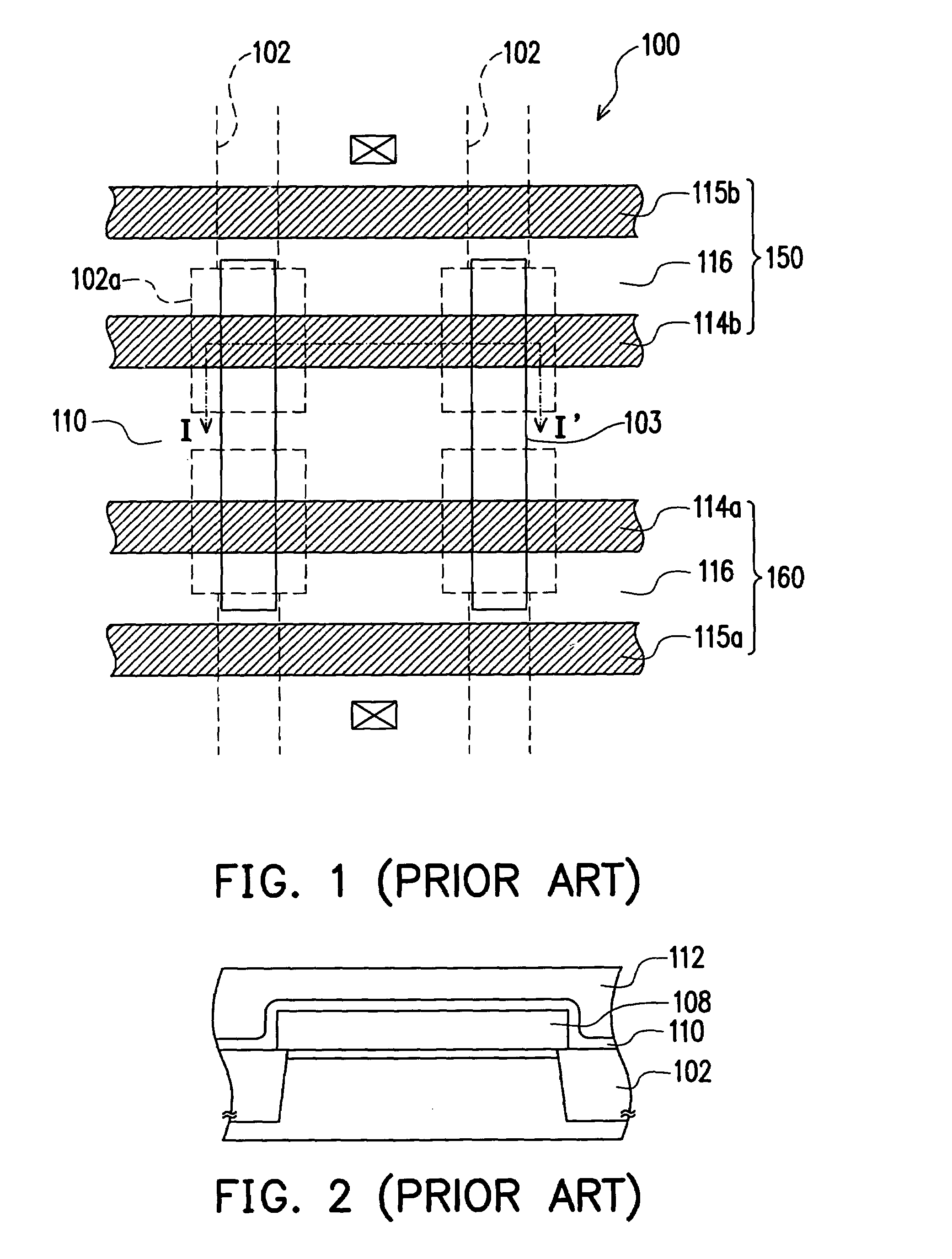
a memory device and memory technology, applied in the field of semiconductor devices, can solve problems such as reliability problems, horizontal two bits, and openings b>103/b> may shift to undesirable positions, and achieve the effects of reducing the distance between memory cells, avoiding misalignment problems, and increasing the reliability of memory devices

Active Publication Date: 2006-06-13
UNITED MICROELECTRONICS CORP
View PDF3 Cites 2 Cited by
  • Summary
  • Abstract
  • Description
  • Claims
  • Application Information

AI Technical Summary

Benefits of technology

[0009]The invention provides a method for fabricating a memory device, of which the isolation structures occupy less active regions. The dimension of the memory cell can be shrunk and the memory device takes less chip areas.
[0010]The invention provides a method for fabricating a memory device, which avoids the problems of varying electrical properties for different memory cells and enhances the reliability for the memory device.
[0012]In the present invention, because the trenches for the isolation structures are etched simultaneously as patterning the first conductive layer and the first dielectric layer, the formed isolation structures are self-aligned with the stacked gate structures, thus increasing the reliability for the memory device by avoiding misalignment problems.
[0013]Moreover, the isolation structures of this invention can be formed in strip shapes, the corner rounding problems therefore can be alleviated and prior problems of unequal electrical properties for different memory cells are avoided even if misalignment occurs. The present invention needs not to preserve greater distances between the corners of the isolation structures and the select gate lines for keeping the select gate lines away from the corners. Thus, distance between the memory cells is efficiently reduced and the areas of the memory cells are effectively decreased.

Problems solved by technology

However, due to many uncontrollable factors of photolithography, corner rounding often occurs to the rectangle isolation structures 102 during the photolithography process.
However, the ONO layer and the polysilicon fence residue near the edge of the patterned first polysilicon layer 108 may result in horizontal two bits and cause reliability problems.
Moreover, once misalignment happens during defining the openings in the first polysilicon layer, the openings 103 may shift to undesirable positions, or even the predetermined location for the select gate line.
Nonetheless, the distance between two adjacent memory cells is increased, leading to consuming more chip areas and preventing the device from having higher level of integration.

Method used


Image

  • Method for fabricating memory device
  • Method for fabricating memory device
  • Method for fabricating memory device

Examples


Embodiment Construction

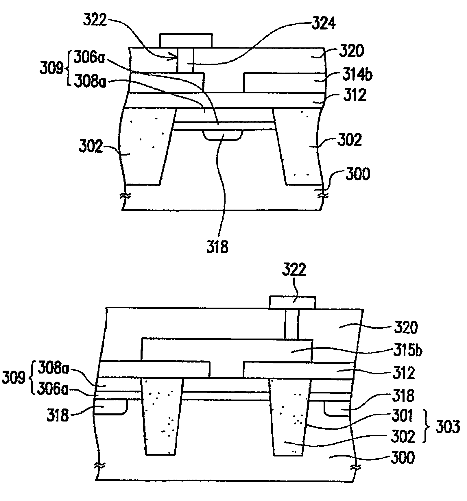
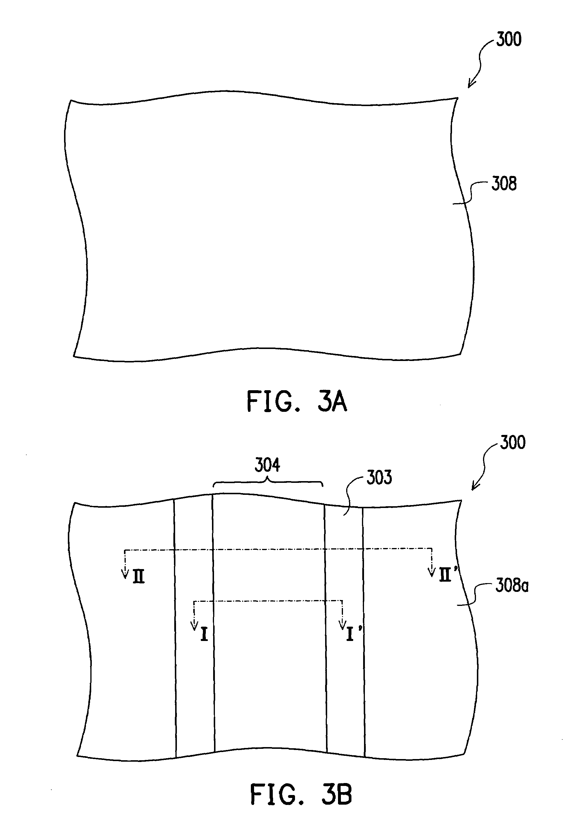
[0021]FIGS. 3A–3D are top views illustrating the process steps for forming a memory structure according to one preferred embodiment of the present invention. FIGS. 4A–4I are cross-sectional views illustrating the process steps for forming the memory structure of FIGS. 3A–3D along the line I–I′, according to one preferred embodiment of the present invention. FIGS. 5A–5K are cross-sectional views illustrating the process steps for forming the memory structure of FIGS. 3A–3D along the line II–II′, according to one preferred embodiment of the present invention.

[0022]Referring to FIGS. 3A, 4A and 5A, a first dielectric layer 306 is formed on the semiconductor substrate 300. The material of the first dielectric layer 306 can be silicon oxide formed by thermal oxidation, for example. A first conductive layer 308 is formed on the first dielectric layer 306 and over the substrate 300. The first conductive layer 308 can be formed by depositing a conductive material layer, for example, a polys...


PUM


Abstract

The present invention relates to a method for fabricating a memory device. According to this invention, because the trenches for the isolation structures are etched simultaneously as patterning the first conductive layer and the first dielectric layer, the formed isolation structures are self-aligned with the stacked gate structures, thus increasing the reliability for the memory device by avoiding misalignment problems.

Description

BACKGROUND OF THE INVENTION[0001]1. Field of Invention[0002]The present invention relates to a semiconductor device and the fabrication method thereof. More particularly, the present invention relates to a method for fabricating a memory device.[0003]2. Description of Related Art[0004]As the flash memories become more developed, they are customarily used in embedded application and sometimes in place of EPROM and EEPROM. The flash memory device allows multiple and repetitive writing, reading and erasure operations, and the storage data are retained even after the power supply is discontinued. Because of the aforementioned advantages, the flash memory has become the mainstream non-volatile memory device, which is widely applied in the electronic products, such as, personal computers, digital cameras and personal digital assistants (PDAs) etc.[0005]At present, the commonly adopted flash memories can be classified as single gate flash memories, split gate flash memories and double gate...

Claims


Application Information

Patent Timeline
Patent Type & Authority Patents(United States)
IPC IPC(8): H01L21/336H01L21/28H01L21/762H01L21/8238H01L27/115
CPCH01L21/28273H01L27/115H01L21/76224H01L29/40114H10B69/00
Inventor LEE, CHEANG
Owner UNITED MICROELECTRONICS CORP
Why Eureka
Try Eureka