Semiconductor device
a technology of semiconductors and devices, applied in semiconductor devices, semiconductor/solid-state device details, electrical apparatus, etc., can solve the problems of thermal deformation of bonding materials, large electrodes, thermal distortion of bonding materials, etc., to improve thermal fatigue life and reduce heat distortion
- Summary
- Abstract
- Description
- Claims
- Application Information
AI Technical Summary
Benefits of technology
Problems solved by technology
Method used
Image

Examples
first embodiment
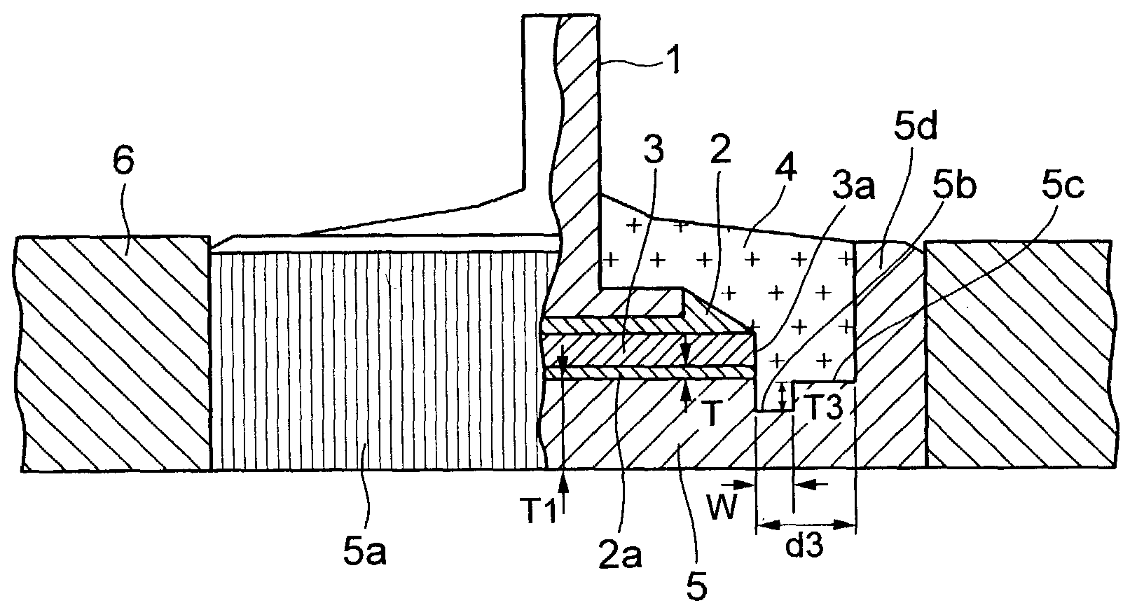
[0038]a semiconductor device according to the invention shown in FIGS. 1 and 2 comprises a lead electrode 1 for connecting with a lead (not shown), a case electrode 5 having a convex wall section 5d at a periphery thereof and a semiconductor chip 3 having a rectification function and placed between the lead electrode 1 and the case electrode 5 through a bonding material 2, 2a. The case electrode 5 includes, in an area between an edge 3a of the semiconductor chip 3 and the convex wall section 5d, a first area 5b which is thinner than the thickness of an area of the case electrode 5 on which the semiconductor chip 3 is placed, and a second area 5c having a thickness which is thicker than that of the first area 5b. The first area 5b is formed so as to extend within a distance five times the thickness of the bonding material 2a bonding the semiconductor chip 3 to the case electrode 5 from the edge 3a of the semiconductor chip 3. In order to improve the heat radiation performance, this s...
third embodiment
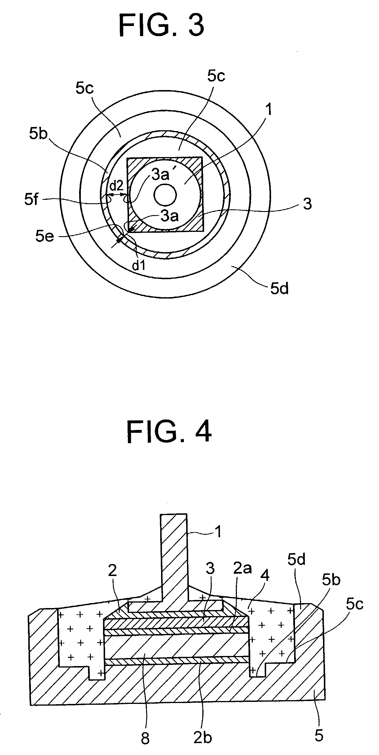
[0045]In the semiconductor device according to the present invention shown in FIG. 4, an intermediate member 8 having a coefficient of linear thermal expansion intermediate those of the semiconductor chip 3 and the case electrode 5 is interposed between the semiconductor chip 3 and the case electrode 5. The intermediate member 8 may be a three-layered structure of copper / iron alloy / copper, for example. With this structure, mechanical stress which is applied to the bonding material 2a and the semiconductor chip 3 is relieved and cracking of the semiconductor chip 3 is prevented.
[0046]The insulating material 4 seals the lead electrode 1, bonding material 2 between the lead electrode 1 and the chip 3, the semiconductor chip 3, the bonding material 2a between the semiconductor chip 3 and the intermediate member 8, the intermediate member 8, a bonding material 2b between the inter-mediate member 8 and the case electrode 5, and the case electrode 5. The insulating material 4 can be made o...
fifth embodiment
[0048]In a semiconductor device according to the present invention shown in FIG. 6, the case electrode 5 and the heat radiation plate 6 are fixed together through the bonding material 2. In comparison with a case in which the case electrode 5 is fixed into a hole in the heat radiation plate 6 having a smaller diameter than that of the case electrode 5 using a press-fitting system, it is to be expected that the amount of stress applied to the case electrode will be reduced.
[0049]A sixth embodiment of a semiconductor device according to the present invention shown in FIG. 7 is similar to the first embodiment. In the sixth embodiment, a height Hb of the convex wall 5d in contact with the heat radiation plate 6 is not greater than a thickness Ha of the heat radiation plate 6 placed on the peripheral side of the case electrode 5. With this structure, when the semiconductor device is mounted inside an engine room of an automobile, it is possible to prevent the case electrode 5 fixed to th...
PUM
 Abstract
Description
Claims
Application Information
 - R&D
- Intellectual Property
- Life Sciences
- Materials
- Tech Scout
- Unparalleled Data Quality
- Higher Quality Content
- 60% Fewer Hallucinations
Browse by: Latest US Patents, China's latest patents, Technical Efficacy Thesaurus, Application Domain, Technology Topic, Popular Technical Reports.
© 2025 PatSnap. All rights reserved.Legal|Privacy policy|Modern Slavery Act Transparency Statement|Sitemap|About US| Contact US: help@patsnap.com