
Multi-scale programmable array

Inactive Publication Date: 2006-06-13
XILINX INC
View PDF35 Cites 20 Cited by
  • Summary
  • Abstract
  • Description
  • Claims
  • Application Information

AI Technical Summary

Benefits of technology

[0012]It is another object of the invention to provide a programmable logic array architecture that allows digital logic to be programmed using both small-scale blocks as well as medium scale blocks.
[0013]It is another object of the invention to provide a programmable logic array architecture that can provide multi-scale functionality and maintain high performance.
[0014]It is another object of the invention to provide a programmable logic array architecture that can achieve fast carry propagation.
[0015]It is another object of the invention to provide a programmable logic array architecture that can provide multi-scale functionality and maintain a single programmable logic element.
[0016]It is another object of the invention to provide a programmable logic array architecture that simplifies the programming of complex arithmetic and random logic functions.
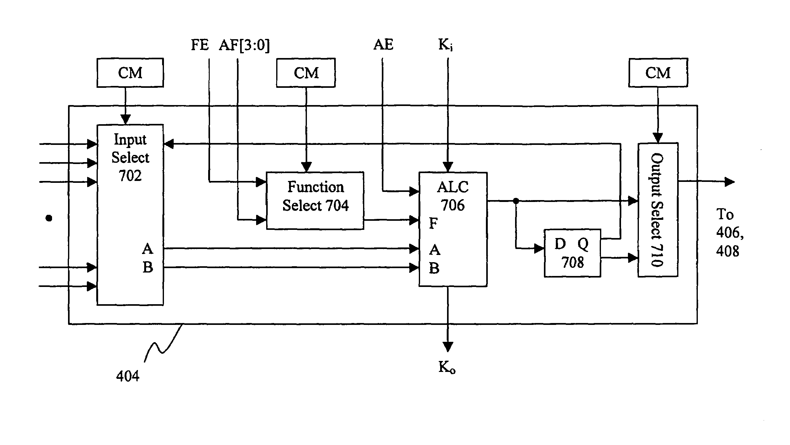
[0019]According to an aspect of the invention, the MSA concept allows digital logic to be programmed using both small-scale blocks (also called gate level blocks) as well as medium scale blocks (also called Register Transfer Level or RTL blocks). Prior art approaches used separate structures to achieve this capability or accepted the reduced performance and increased cost of having a single programmable logic type. The MSA concept is based on a bit sliceable Arithmetic Logic Unit (ALU). Each bit-slice may be programmed to perform a basic Boolean logic operation or to contribute to higher-level functions that are further programmed by an ALU controller circuit. In one embodiment of the invention, the ALU controller level also allows the primitive logic operations computed at the bit-slice level to be combined to perform complex random logic operations. The data shifting capability of this new programmable logic architecture according to another aspect of the invention reduces the complexity of the programmable routing needed to implement shift operations including multiplier arrays. The new array also allows logic variables under program control to dynamically modify the micro-program of each ALU. This technique is called configuration overlay and simplifies the programming of complex arithmetic and random logic functions.

Problems solved by technology

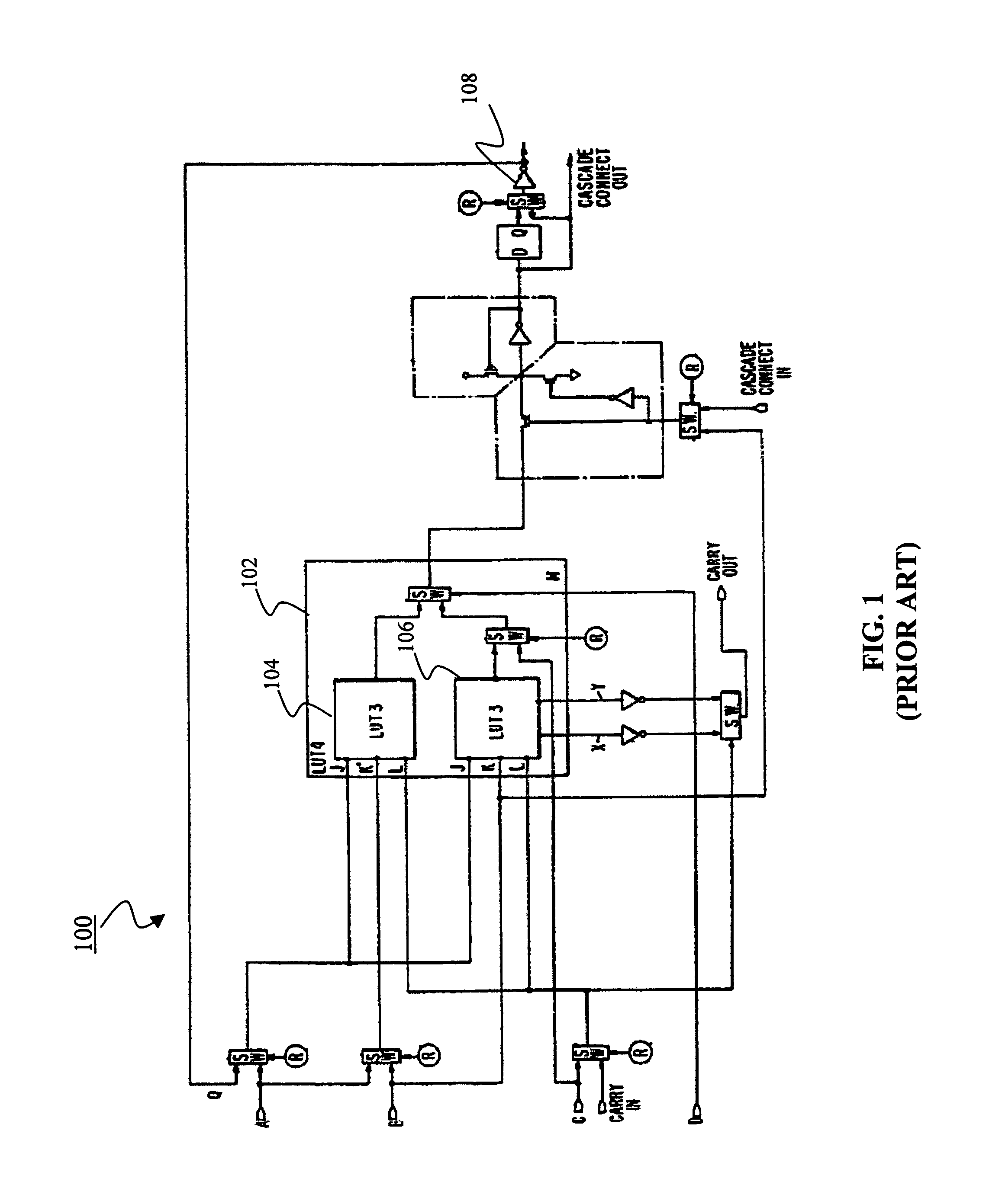
For example, when attempting to program structures for performing higher-level functions (such as arithmetic and complex logic operations), many logic elements are required to be combined together, which leads to larger structures and reduced performance, including slow carry propagation.
Further, to allow logic elements to be combined together to perform expanded logic operations, combinational logic must be included in each element, even when such operations are not programmed, thus leading to wasteful circuitry.
Moreover, the prior art structures can only be statically programmed to perform different levels of functionality.

Method used


Image

  • Multi-scale programmable array
  • Multi-scale programmable array
  • Multi-scale programmable array

Examples


Embodiment Construction

[0044]FIG. 3 illustrates a multi-scale programmable logic array (MSA) 300 in accordance with the principles of the present invention. As shown, array 300 includes a plurality of cluster blocks 302 arranged in rows and columns. Data is communicated between cluster blocks 302 by means of a global interconnect 304. As shown, the global interconnect 304 also communicates data and dynamic configuration information used or output by array 300 with other devices, which data and dynamic configuration information will be described in more detail below. Although generically shown as permitting any two cluster blocks 302 in array 300 to communicate directly with each other via interconnect 304, such interconnections need not be so limited. For example, cluster blocks 302 can additionally or alternatively have interconnections such that blocks in adjacent rows and / or columns communicate directly with each other.

[0045]Although not necessarily part of array 300, and preferably separately provided...


PUM


Abstract

A novel architecture for a multi-scale programmable logic array (MSA) to be used in the design of complex digital systems allows digital logic to be programmed using both small-scale blocks (also called gate level blocks) as well as medium scale blocks (also called Register Transfer Level or RTL blocks). The MSA concept is based on a bit sliceable Arithmetic Logic Unit (ALU). Each bit-slice may be programmed to perform a basic Boolean logic operation or may be programmed to contribute to higher-level functions that are further programmed by an ALU controller circuit. The ALU controller level in this new approach also allows the primitive logic operations computed at the bit-slice level to be combined to perform complex random logic operations. The data shifting capability of this new programmable logic architecture reduces the complexity of the programmable routing needed to implement shift operations including multiplier arrays. The new array also allows logic variables under program control to dynamically modify the micro-program of each ALU. This technique is called configuration overlay and simplifies the programming of complex arithmetic and random logic functions.

Description

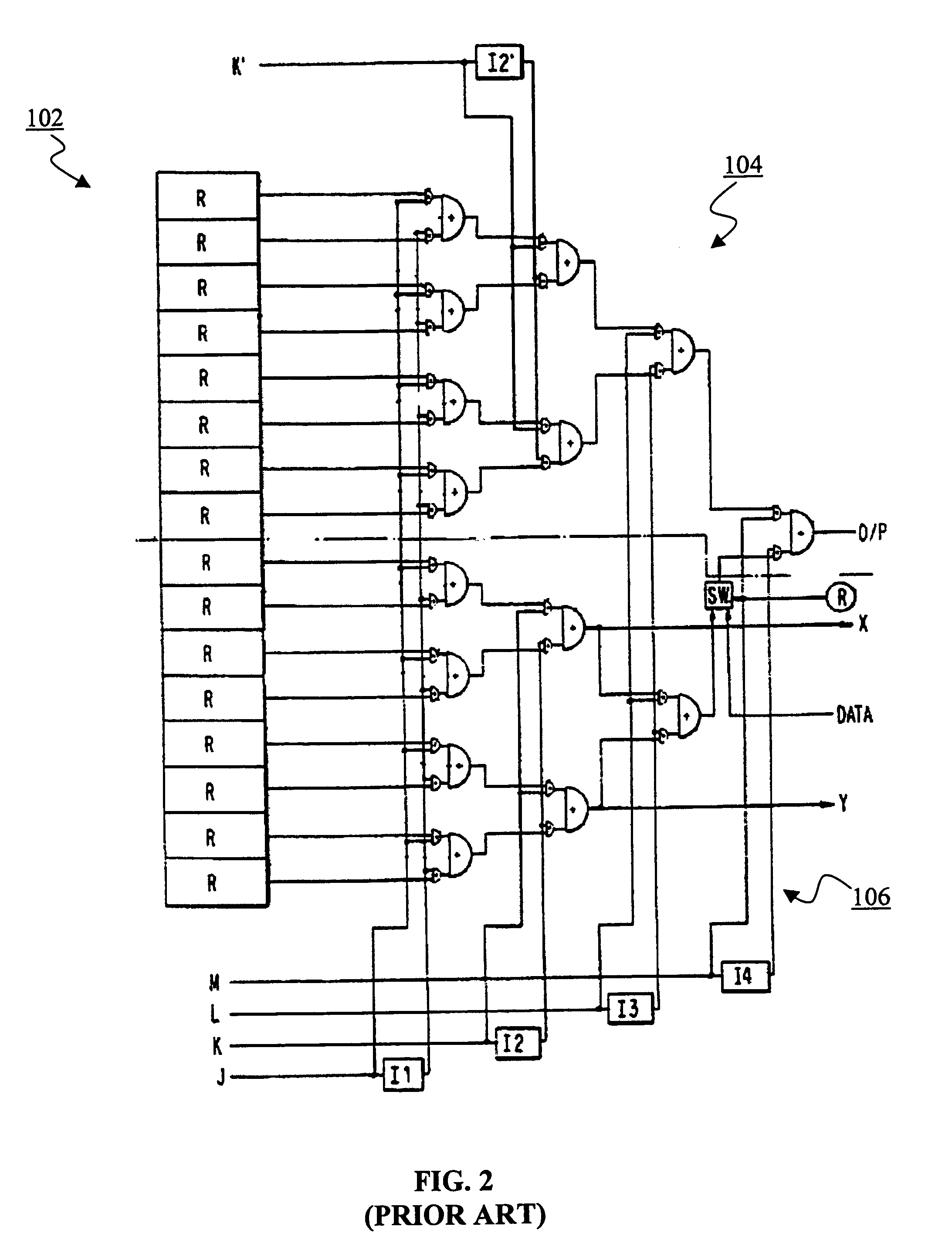
[0001]This is a continuation of Application Ser. No. 09 / 475,400, filed Dec. 30, 1999.BACKGROUND OF THE INVENTION[0002]1. Field of the Invention[0003]The present invention relates to the field of Programmable Logic Arrays (PLAs), Field Programmable Gate Arrays (FPGAs) and Programmable Logic Devices (PLDs). More particularly, the present invention relates to a programmable logic array architecture in which individual logic elements are based on a bit sliceable arithmetic logic unit (ALU), each bit slice being individually programmable to perform low-level Boolean and gate-level operations, as well as higher-level logic and arithmetic functions.[0004]2. Description of the Related Art[0005]FIG. 1 illustrates a programmable logic element 100 used in a conventional programmable logic device. Typically, a logic device includes a two-dimensional array of elements such as element 100 disclosed in U.S. Pat. No. 5,274,581.[0006]As shown, element 100 implements a four-input look-up table 102 wh...

Claims


Application Information

Patent Timeline
IPC IPC(8): G06F7/38H03K19/177
CPCH03K19/17796H03K19/17728
Inventor RUPP, CHARLE' R.
Owner XILINX INC
Learn More