
Mass storage device architecture and operation

a mass storage device and architecture technology, applied in the field of mass storage devices, can solve the problems of increasing die size, reducing the performance level of a receiving device, and requiring high-cost control circuitry to achieve the desired performance level, etc., to achieve fast read throughput, support overhead time reduction, and reduce the effect of first bit latency

Active Publication Date: 2006-06-13
INFINEON TECH AG +1
View PDF8 Cites 16 Cited by
  • Summary
  • Abstract
  • Description
  • Claims
  • Application Information

AI Technical Summary

Benefits of technology

The present invention provides an improved chip architecture for a mass storage device that reduces first bit latency and increases read throughput. It also allows for simultaneous performance of an internal operation and program verify cycles, and enables program operations without a need for an additional second buffer. The device includes a data buffer and a data path unit with a master buffer and a main data bus. The main data bus is designed to transfer data between the data path unit and an input / output unit via a buffer interface unit comprising a plurality of slave buffers. The device also includes a redundant portion dedicated to store data that is supposed to be stored in other parts of the device. The method of operation involves performing an internal operation while in parallel performing an internal read access to the device. The invention also includes a method for performing a boolean operation on binary integers to determine which bits in the device need to be programmed. Overall, the invention improves the speed and efficiency of mass storage devices.

Problems solved by technology

However, this may have the disadvantage of significant system overhead, thereby reducing the performance level of a receiving device, or alternatively, requiring high cost control circuitry to achieve the desired performance level.
Such a method requires two separate buffers and increases the die size.

Method used


Image

  • Mass storage device architecture and operation
  • Mass storage device architecture and operation
  • Mass storage device architecture and operation

Examples


Embodiment Construction

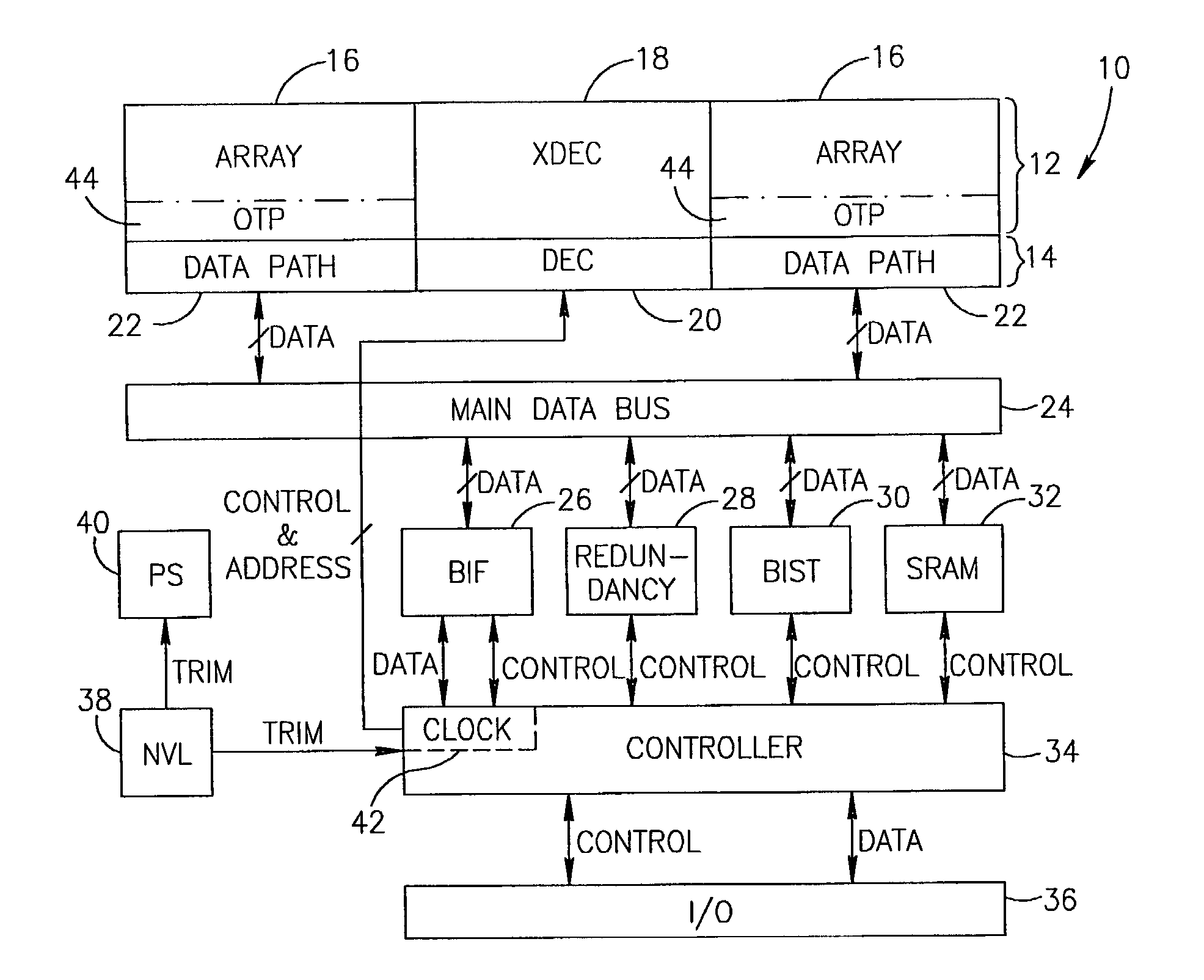
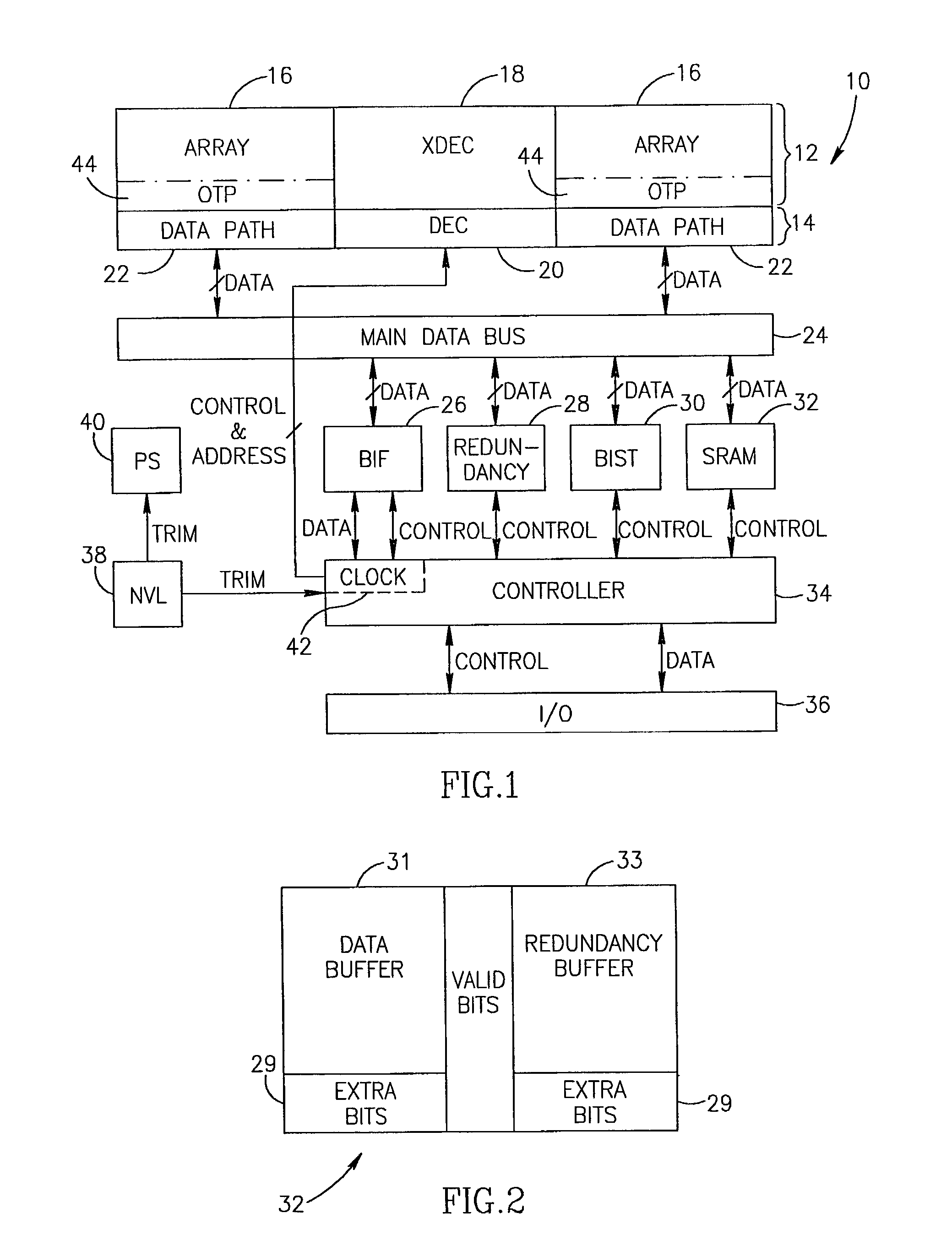
[0051]Reference is now made to FIG. 1, which illustrates a mass storage device 10, constructed and operative in accordance with a preferred embodiment of the present invention.

[0052]In accordance with an embodiment of the invention, the mass storage device 10 may comprise a NVM core 12 and periphery 14. The core 12 may comprise one or more banks of memory cell arrays 16, such as but not limited to, having a size of 0.5 Gb (for exemplary purposes only). In the illustrated embodiment there are two such arrays 16, both served by an X-decoder (XDEC) 18, however, the invention is not limited to this amount of arrays. Memory cell arrays 16 may comprise nitride, read-only memory (NROM) cells, and the array architecture may comprise a mass storage NROM array architecture as described in U.S. Patent Application No. 60 / 352,589, assigned to the present assignee, the disclosure of which is incorporated herein by reference. The XDEC 18 may be located between the arrays 16 to conserve space. The ...


PUM


Abstract

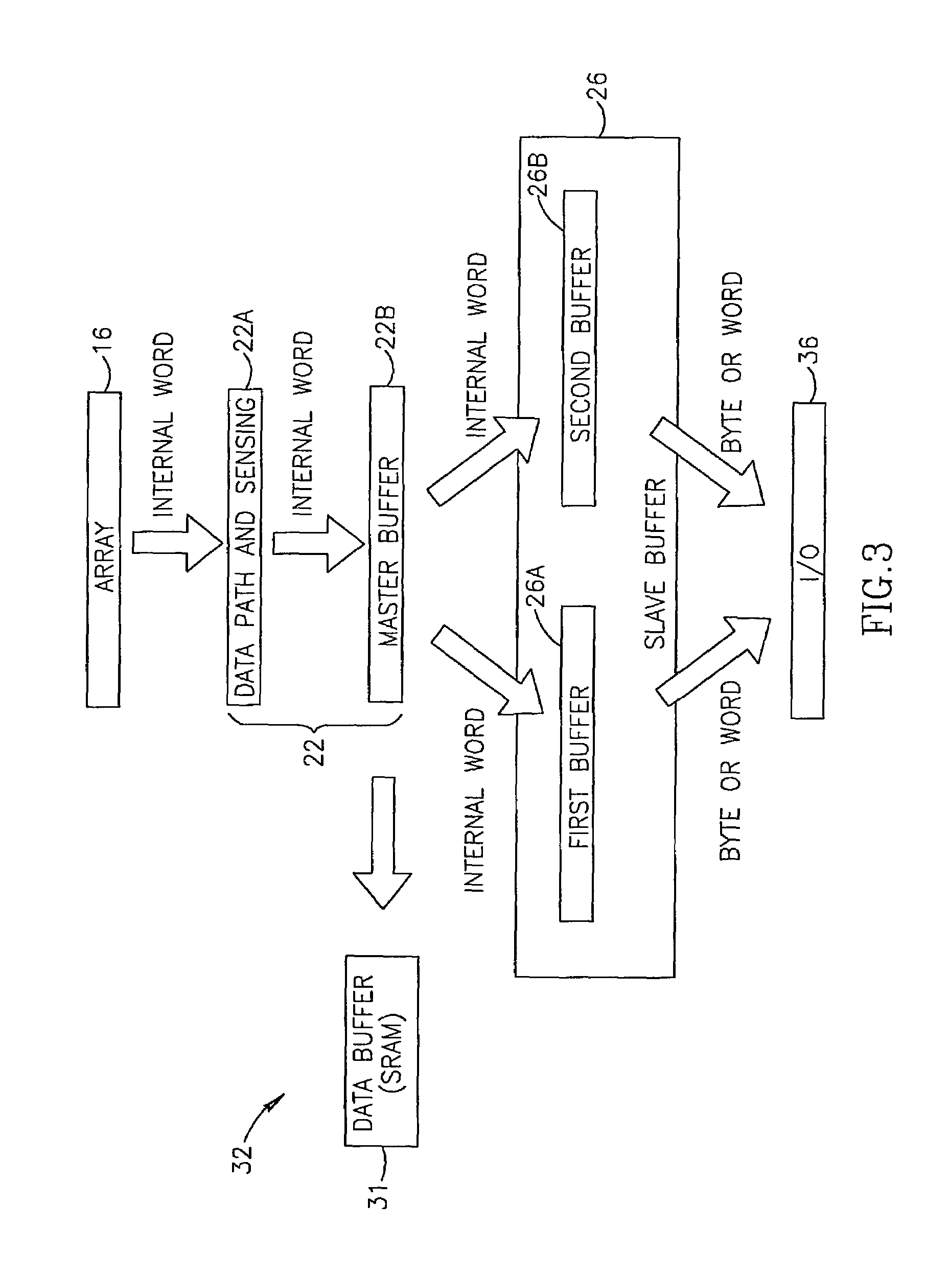
A mass storage device comprising at least one array of memory cells, at least one data path unit in communication with the at least one array, the at least one data path unit comprising a master buffer, and a main data bus adapted to transfer data between the at least one data path unit and an input / output (I / O) unit via a buffer interface unit (BIF) comprising a plurality of slave buffers, the main data bus being further adapted to support at least one of a download and upload of data between the main data bus and the I / O unit, during simultaneous performance of an internal operation between the main data bus and the at least one array, the internal operation comprising at least one of a read, program and erase operation. Methods for operating the mass storage device are also disclosed.

Description

CROSS-REFERENCE TO RELATED APPLICATIONS[0001]The present application claims priority from U.S. provisional application Ser. No. 60 / 352,588, filed Jan. 31, 2002, which is hereby incorporated by reference in its entirety.FIELD OF THE INVENTION[0002]The present invention relates generally to mass storage devices, and particularly to architectures for mass storage devices that include non-volatile memory cell arrays and cache memory.BACKGROUND OF THE INVENTION[0003]Mass storage non-volatile memory (NVM) devices enable read and / or write access to data containing many bytes. Mass storage devices are typically, but not only, used in applications such as hard disks, or digital video storage devices, such as for digital cameras. Throughout the specification and claims, the term “mass storage device” refers not only to memory devices that are capable of the storage functionality of hard disks or video storage devices and the like, but also to memory devices capable of storing and providing ac...

Claims


Application Information

Patent Timeline
Patent Type & Authority Patents(United States)
IPC IPC(8): G06F12/00G11C7/10G11C29/00
CPCG11C7/1051G11C7/106G11C7/1087G11C7/1078G11C2207/2245G11C29/70
Inventor DVIR, RANCOHEN, ZEEVMAAYAN, EDUARDO
Owner INFINEON TECH AG
Learn More