Method of fixing space defining members in an envelope of an electron beam apparatus
- Summary
- Abstract
- Description
- Claims
- Application Information
AI Technical Summary
Benefits of technology
Problems solved by technology
Method used
Image

Examples
embodiment 1
(Embodiment 1)
[0115]In this embodiment, a display panel corresponding to the first embodiment mode is manufactured.
[0116]A glass which has a length of 200 [mm], a width of 5 [mm], and a thickness of 0.2 [mm] and is the same as the glass for the rear plate 15 is prepared for an insulating member 20a of each of spacers. As for a high resistance film, simultaneous sputtering using targets of W and Ge is conducted in an atmosphere in which argon and nitrogen are mixed with each other by a sputtering apparatus, so that a nitride film containing W and Ge is laminated at a thickness of 200 [nm]. A resistivity of the formed nitride film containing W and Ge is 5.0×10⁵ [Ωm]. Next, low resistance films (electrodes) are formed on the surface of each of the spacers 20 which is in contact with the rear plate 15 and the surface of each of the spacers 20 which is in contact with the face plate 17.
[0117]Here, the low resistance films are used to electrically connect the high resistance film 20b with...
embodiment 2
(Embodiment 2)
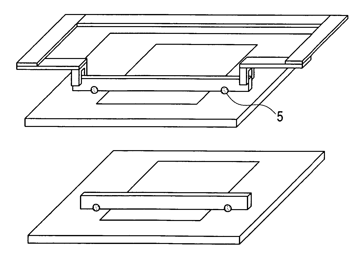
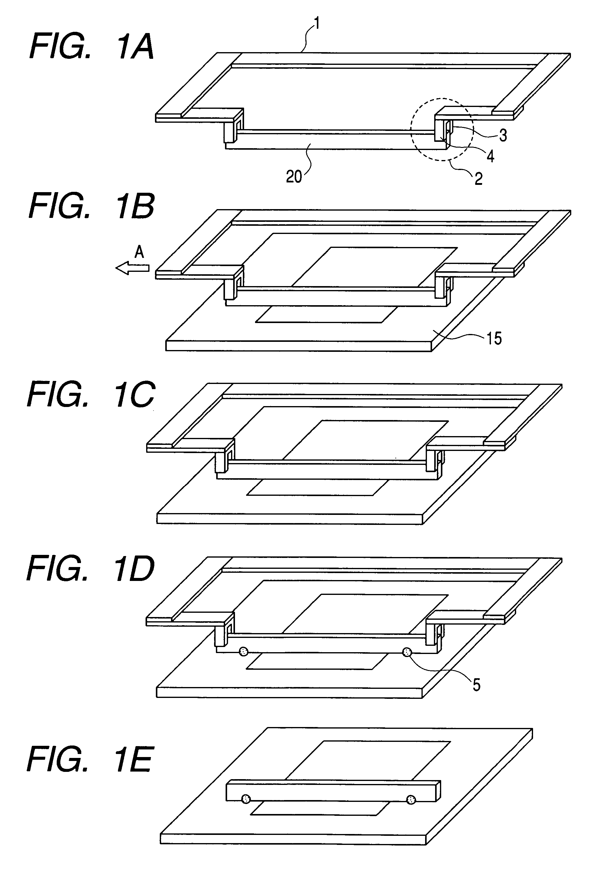
[0122]A display device having the same structure as that of Embodiment 1 above is produced. At this time, each of the spacers 20 has the auxiliary support members 6 in both ends thereof. In addition, the spacers 20 are provided to the rear plate 15 by the method described above with reference to FIGS. 2A to 2E. The other structure is identical to that of Embodiment 1. In this embodiment, as in Embodiment 1, light emission spot arrays including light emission spots due to the emitted electrons from the cold cathode devices 12 located near the spacers 20 are two-dimensionally produced at regular intervals. Accordingly, a color image which is sharp and has preferable color reproducibility can be displayed.
embodiment 3
(Embodiment 3)
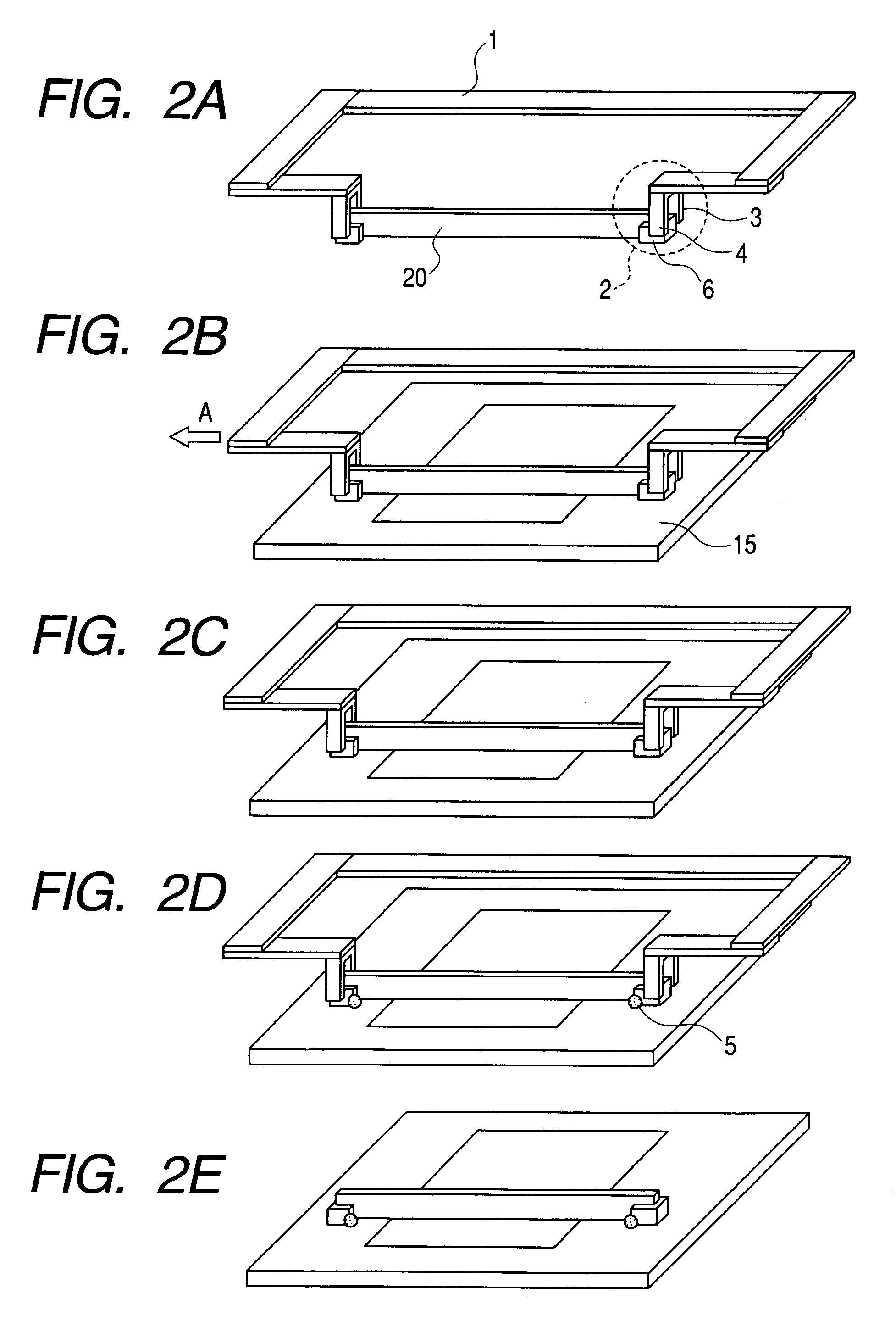
[0123]A display device having the same structure as in Embodiment 1 above is produced. At this time, each of the spacers 20 has the auxiliary support members 6 in both ends thereof. In addition, the spacers 20 are provided to the rear plate 15 by the method described above with reference to FIGS. 3A to 3F. The other structure is identical to that in Embodiment 1. In this embodiment, as in Embodiment 1, light emission spot arrays including light emission spots due to the emitted electrons from the cold cathode devices 12 located near the spacers 20 are two-dimensionally produced at regular intervals. Accordingly, a color image which is sharp and has preferable color reproducibility can be displayed.
[0124]As described above, according to the present invention, the spacers are easy to locate and a displacement of each of the spacers can be prevented to improve the assembly accuracy. Thus, an envelope or an electron beam apparatus for an image display device can be manufac...
PUM
 Abstract
Description
Claims
Application Information
 - R&D
- Intellectual Property
- Life Sciences
- Materials
- Tech Scout
- Unparalleled Data Quality
- Higher Quality Content
- 60% Fewer Hallucinations
Browse by: Latest US Patents, China's latest patents, Technical Efficacy Thesaurus, Application Domain, Technology Topic, Popular Technical Reports.
© 2025 PatSnap. All rights reserved.Legal|Privacy policy|Modern Slavery Act Transparency Statement|Sitemap|About US| Contact US: help@patsnap.com