Ferromagnetic-semiconductor composite isolator and method

a composite isolator and magnetosemiconductor technology, applied in the direction of optical elements, optical waveguide light guides, instruments, etc., can solve the problems of complex manufacture and implementation high cost and complexity of conventional optical isolators, and inability to meet the requirements of high-efficiency optical isolators, etc., to achieve reliable and efficient interfacing, reduce overall cost, and improve reliability and cost

Inactive Publication Date: 2006-06-20
KELTON CAPITAL L L C
View PDF4 Cites 15 Cited by
  • Summary
  • Abstract
  • Description
  • Claims
  • Application Information

AI Technical Summary

Benefits of technology

[0013]Another technical advantage of the present invention includes the capability to use existing and available manufacturing techniques and processes, including, for example, conventional semiconductor fabrication processes, to fabricate and implement certain embodiments of the invention. This further reduces overall costs to implement and practice the present invention.
[0014]Another technical advantage of the present invention includes the capability to reliably and accurately manufacture optical isolators that provide known and predetermined optical isolation properties, while reliably and efficiency interfacing with other semiconductor optical elements, such as semiconductor lasers, optical processors and other conventional optical elements.
[0015]Yet another technical advantage of the present invention includes the capability to integrate external optical isolators into existing optical semiconductor devices to provide superior overall device and system performance, reliability, cost, while also reducing overall device and system weight, volume and operational complexity.
[0016]Other technical advantages are readily apparent to one skilled in the art from the following figures, description, and claims.

Problems solved by technology

The presence of reflected light waves in such systems and networks are problematic and may result in significant problems, disadvantages and instabilities, especially when reflected light waves reach or reenter a laser source, such as a semiconductor laser, or optical amplifier.
Unfortunately, the manufacture and implementation of conventional optical isolators is complicated, unreliable, expensive and fraught with difficulties and disadvantages.
The implementation of conventional optical isolators is often cumbersome and expensive.
This phase match requirement of conventional optical isolators with their light source, such as a semiconductor laser, is particularly difficult and problematic, and imposes severe fabrication tolerances.
For example, the fabrication tolerances on such variables as composition, layer thickness, and interaction length are extremely difficult to consistently achieve and replicate.
This causes reliability and performance concerns, along with significantly increased overall costs.
This has presented serious challenges and problems.
The dramatically different fabrication techniques and materials used in semiconductor optical elements and conventional optical elements and devices has made integration of these optical elements and devices either impossible or impractical.

Method used


Image

  • Ferromagnetic-semiconductor composite isolator and method
  • Ferromagnetic-semiconductor composite isolator and method
  • Ferromagnetic-semiconductor composite isolator and method

Examples


first embodiment

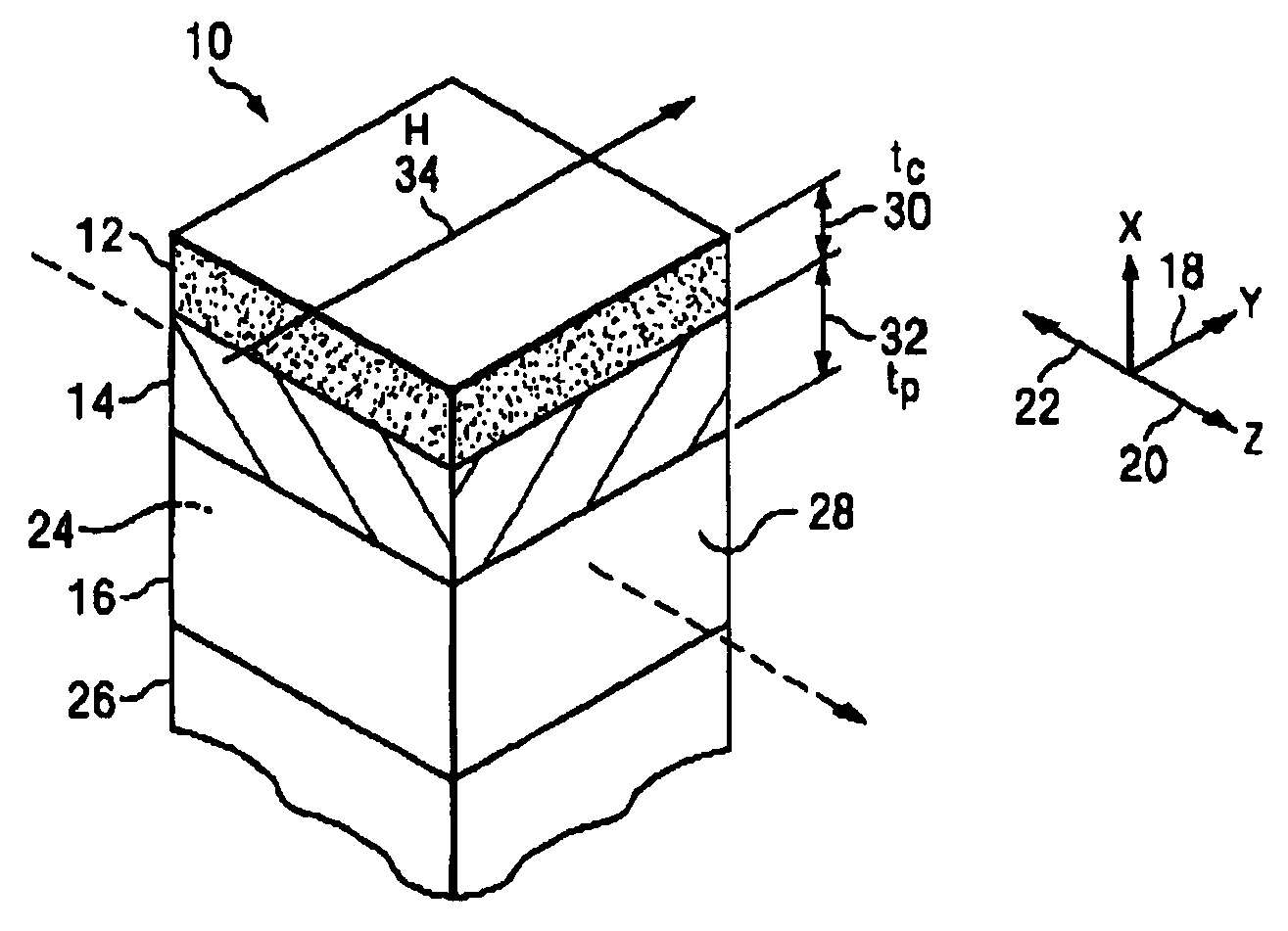
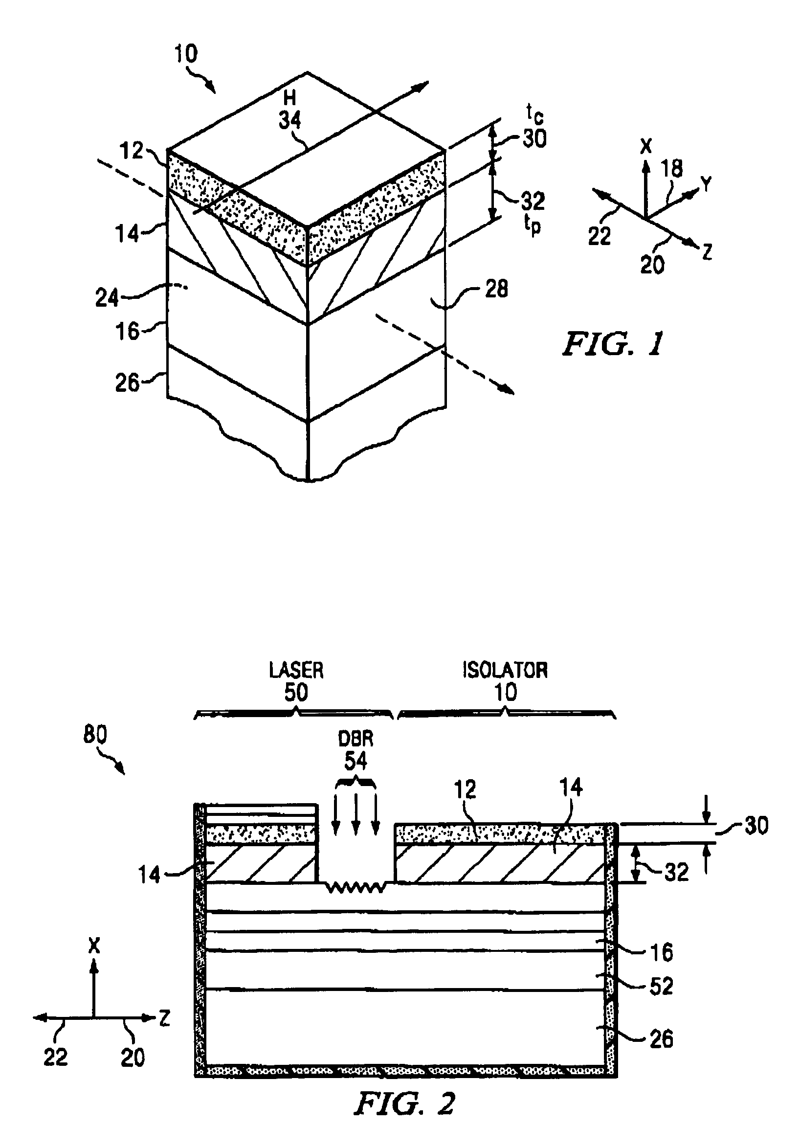
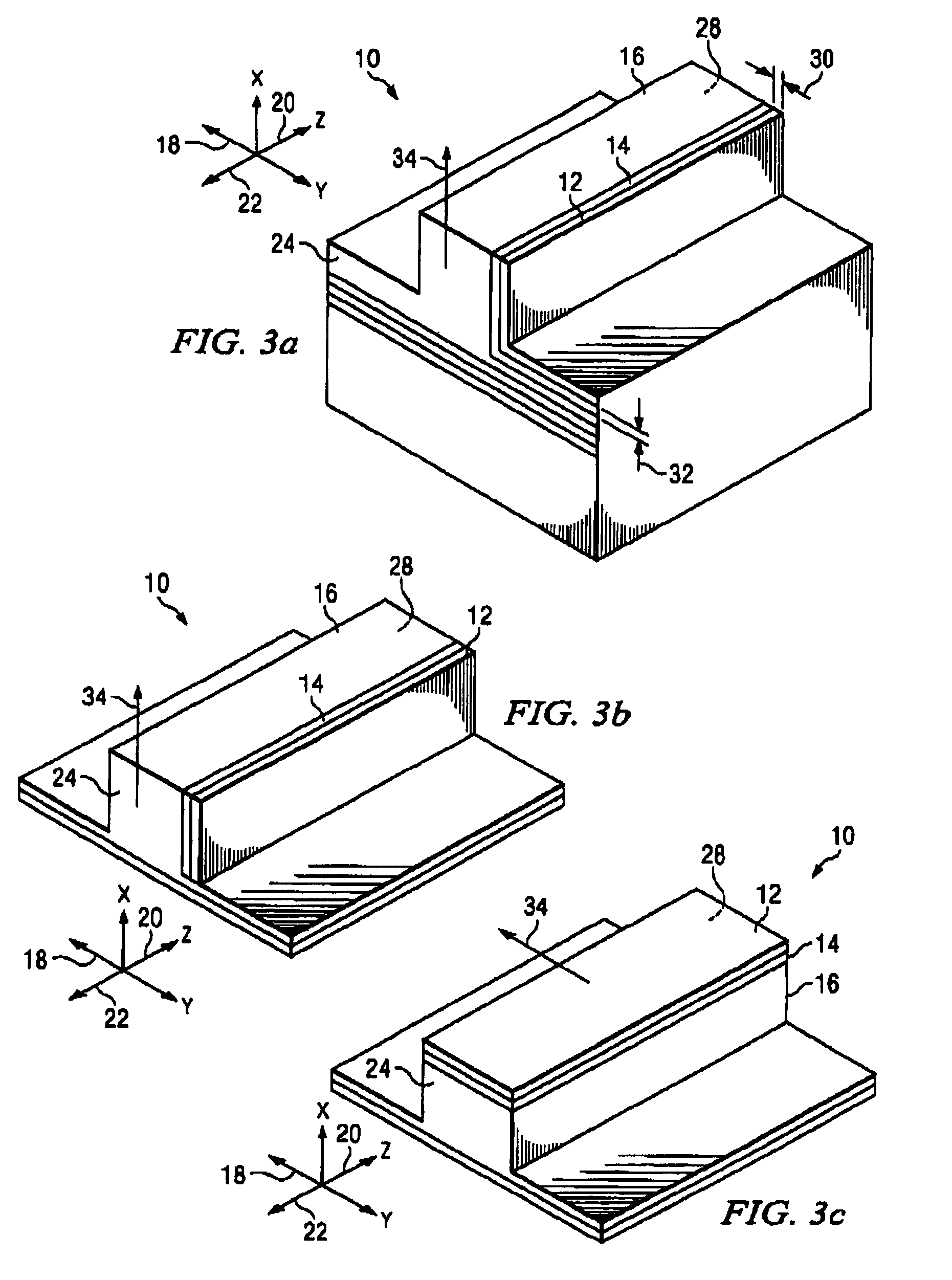
[0056]Two examples or embodiments of the FC layer 12 are provided below. The first embodiment uses an FC layer 12 with iron particles in GaAs deposited on the p-cladding of the second clad layer 14 of a multi-quantum well laser type structure with layers as listed in Table 1 below for operation at a wavelength of 1.3 μm (nm). At this wavelength, GaAs has a refractive index of 3.45 which is higher than the refractive index of the p-clad of AlInAs of the second clad layer 14, which is 3.231. These values satisfy the need to have the material of the FC layer 12 in which the iron particles are positioned with a refractive index equal to or greater than that of the p-clad of the second clad layer 14. The cutoff thickness for the FC layer 12 is shown in Table 3 below.

[0057]At a second clad layer 14 p-clad thickness of tp=3.0 μm and an FC layer 12 thickness tc=0.32, the isolation is 111 dB / cm with insertion loss of only 6.3 dB / cm giving the excellent isolation-to-loss ratio of 17.6 in unit...

second embodiment

[0066]the FC layer 12 for operation at a wavelength λ of 1.55 μm is described next. In this embodiment, the FC layer 12 uses iron particles in silicon deposited on the p-cladding of a multi-quantum well laser structure with layers as listed below in Table 2. The thickness 30 of the FC layer 12 and the minimum thickness 32 of the p-clad layer of the second clad layer 14 is determined as described above. At λ=1.55 μm, silicon had a refractive index of 3.4 and the p-clad of InP has a refractive index=3.163. These values satisfy the need to have the semiconductor material of the FC layer 12 with an index of refraction equal to or greater than the index of refraction of the p-clad layer 14. The cutoff thickness for the FC layer 12 is shown below in Table 3.

[0067]

TABLE 2An Isolator using Fe-Silicon FC layer 12 deposited on a typicalMQW structure is using quaternary semiconductor layers foroperation in the 1.55 μm region. This can be fabricated on thesame material as a laser or amplifier. ...


PUM

PropertyMeasurementUnit
thicknessaaaaaaaaaa
thicknessaaaaaaaaaa
thicknessaaaaaaaaaa

Abstract

An exemplary optical isolator, such as a magnetic-semiconductor composite optical isolator, and method for making the same, is provided that includes a semiconductor waveguide and a magnetic-semiconductor composite layer. The semiconductor waveguide includes a guide layer, a first clad layer and a second clad layer. The guide layer includes one or more layers with a first end, a second end, a top, and a bottom, the guide layer allows a light wave incident the first end of the guide layer to propagate in a positive propagation direction, and allows a light wave incident the second end of the guide layer to propagate in a negative propagation direction. The first clad layer and the second clad layer are provided, respectively, relative to the bottom and the top of the guide layer, and the second clad layer has a thickness to allow an optical field penetration through the second clad layer. The magnetic-semiconductor composite layer is provided in the presence of a magnetic field oriented in a desired direction and is positioned relative the second clad layer and at a thickness and index of refraction to receive the optical field penetration through the second clad layer and to attenuate a light wave that propagates in the negative propagation direction more than the attenuation of a light wave that propagates in the positive propagation direction. The magnetic-semiconductor composite optical isolator may be integrated with a semiconductor laser, such as on the same semiconductor substrate.

Description

CROSS-REFERENCE TO RELATED APPLICATIONS[0001]Pursuant to 35 U.S.C. § 119(e), this application claims the benefit of U.S. Provisional Patent Application Ser. No. 60 / 451,160, entitled Ferromagnetic-Semiconductor Composite Isolator and Method, filed Jul. 7, 2003, and named Jacob M. Hammer as inventor, which is hereby incorporated by reference for all purposes.TECHNICAL FIELD OF THE INVENTION[0002]This invention relates in general to the field of semiconductor lasers and optical isolators and more particularly to a ferromagnetic-semiconductor composite optical isolator and method.BACKGROUND OF THE INVENTION[0003]Optical isolators are used in optical communications systems and optical networks to eliminate or reduce reflected light waves. The presence of reflected light waves in such systems and networks are problematic and may result in significant problems, disadvantages and instabilities, especially when reflected light waves reach or reenter a laser source, such as a semiconductor la...

Claims


Application Information

Patent Timeline
Patent Type & Authority Patents(United States)
IPC IPC(8): G02B6/00G01N21/01G02B21/34G02F1/00G02F1/03G02F1/07G02F1/09G02F1/095
CPCG02F1/0036G02F1/0955G02F1/091
Inventor HAMMER, JACOB M.
Owner KELTON CAPITAL L L C
Why Eureka
Try Eureka