

Flip-chip light emitting diode and fabricating method thereof
a light-emitting diode and flip-chip technology, applied in semiconductor devices, electrical equipment, semiconductor/solid-state device testing/measurement, etc., can solve the problems of reducing the light output intensity of flip-chip led, unable to be a light output source, and absorbing light emitted upward from the flip-chip led by the substrate, so as to achieve the effect of greatly improving the product quality and brightness of the led and efficient increase the light output intensity
- Summary
- Abstract
- Description
- Claims
- Application Information
AI Technical Summary
Benefits of technology
Problems solved by technology
Method used
Image

Examples
embodiment 1
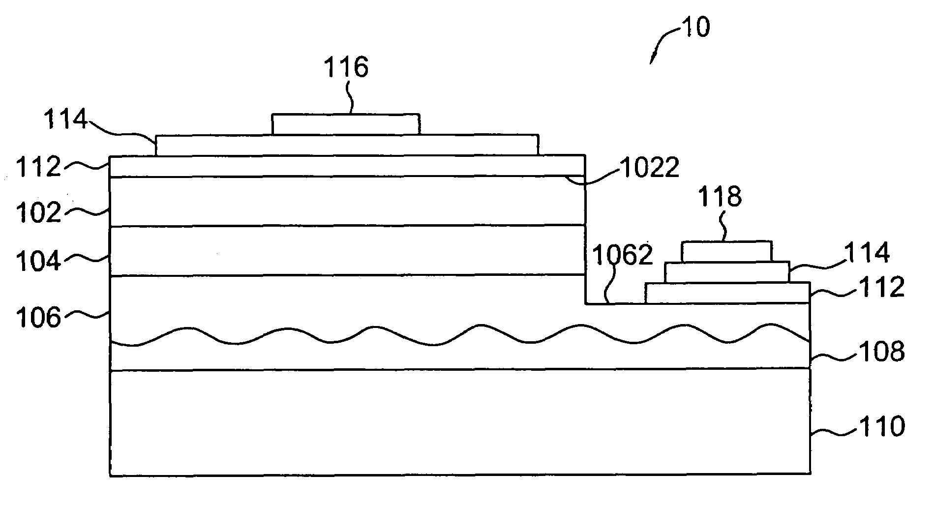
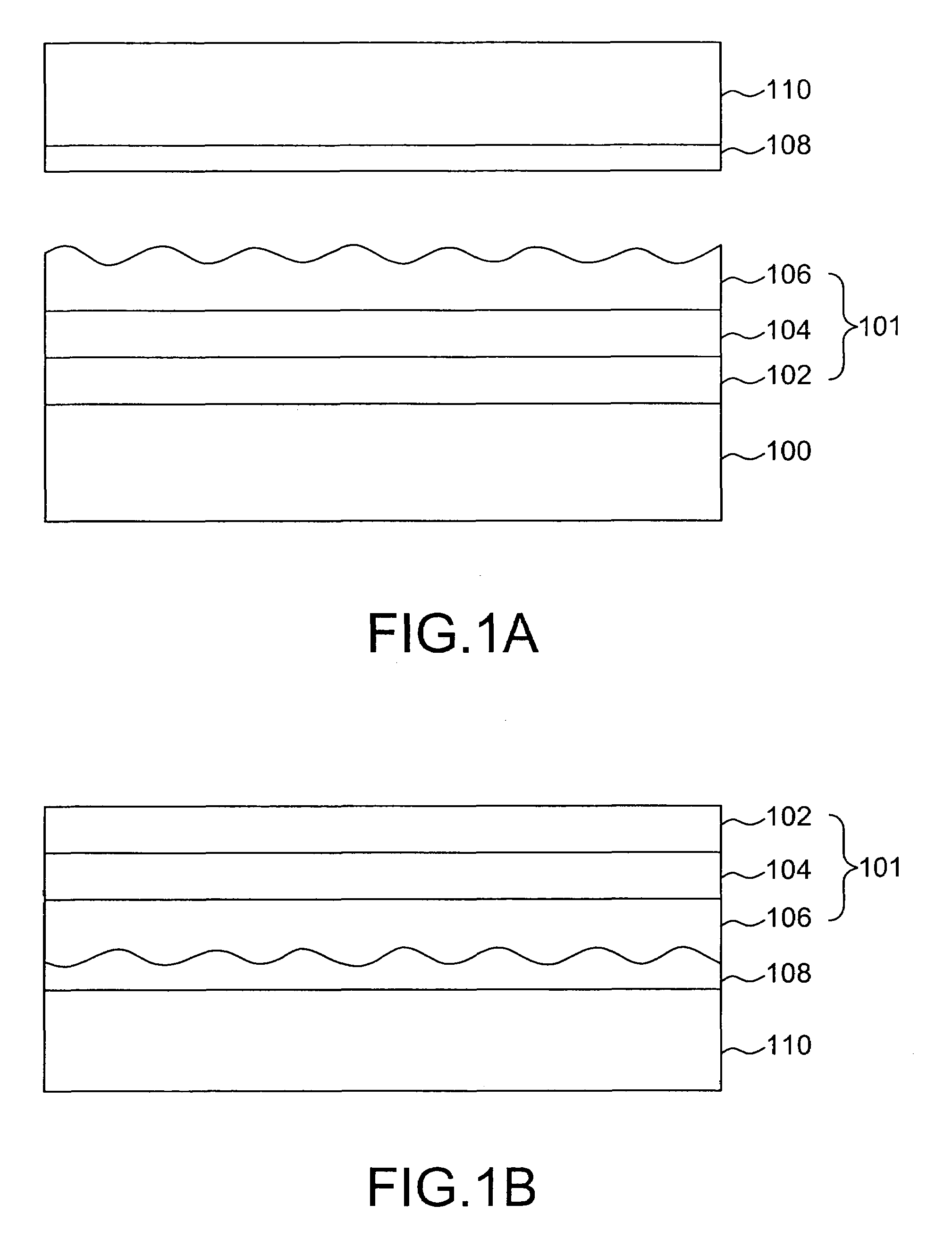
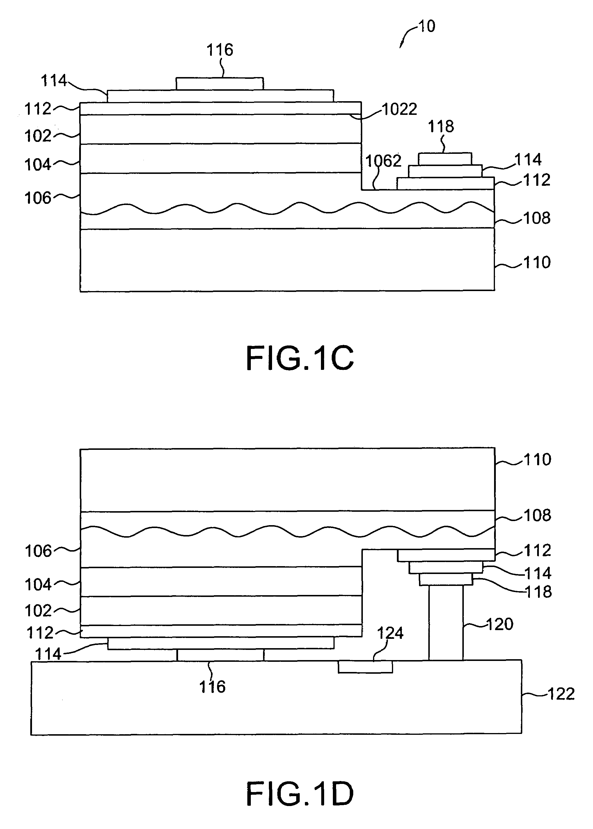
[0022]A flip-chip LED 10 is disclosed in accordance with the present invention. FIGS. 1A–1D are cross-sectional, schematic diagrams showing the process for forming the flip-chip LED 10 in accordance with the preferred embodiment of the present invention.
[0023]In FIG. 1A, an LED epitaxy structure 101 is first formed on a substrate 100. The LED epitaxy structure 101 mentioned herein includes an AlGaInP LED epitaxy structure and an AlGaInN LED epitaxy structure. To obtain an epitaxy structure of high quality, the selected material of the substrate 100 corresponding to the AlGaInP LED epitaxy structure is Ge, GaAs or InP. As for the AlGaInN LED epitaxy structure, the preferred material of the substrate 100 is sapphire, SiC, Si, LiAlO2, ZnO or GaN. The LED epitaxy structure 101 is fabricated by forming an n-type semiconductor layer 102, an active layer 104, and a p-type semiconductor layer 106 on the substrate 100. Further, the surface of the p-type semiconductor layer 106 is next roughe...
embodiment 2
[0032]FIG. 2 shows a resulting structure of flip-chip LED 20 in accordance with the preferred embodiment of the present invention. With reference to FIG. 2 in which like reference numerals refer to like feature in FIGS. 1A–1D, and at a subsequent fabrication, the upper surface of the transparent substrate 210 is roughened to form a rough surface for improving the light output intensity, and the brightness of LED 20 is increased.
[0033]Moreover, not only the interface of the transparent substrate 210 and the soft transparent adhesive layer 208, but also the lower surface of the transparent substrate 210 is formed with roughness property.
[0034]The upper and lower surface of the transparent substrate 210 are either roughened before the soft transparent adhesive layer 208 is coated or by micro-etching the surface of transparent substrate 210 after the transparent substrate 210 is adhered to the p-type semiconductor layer 206.
embodiment 3
[0035]FIGS. 3A–3D are cross-sectional, schematic diagrams showing the process for forming the flip-chip LED 30 in accordance with the preferred embodiment of the present invention.
[0036]The LED epitaxy structure 301 shown in FIG. 3A is fabricated by forming an n-type semiconductor layer 302, an active layer 304, and a p-type semiconductor layer 306 on the substrate 300 in accordance with the manufacturing steps of Embodiment 1. The active layer 304 of this embodiment (Embodiment 3) is similar to the active layer 104 of Embodiment 1, i.e. the active layer 304 may be a homo-structure, single hetero-structure, double hetero-structure, or multi-quantum well structure (MQW).
[0037]A temporary substrate 310 having a surface coated with a soft transparent adhesive layer 308 is then bonded to the LED epitaxy structure 301, in which the temporary substrate 310 is pasted down on the p-type semiconductor layer 306 by the adhesion property of the soft transparent adhesive layer 308. The temporar...
PUM
 Abstract
Description
Claims
Application Information