
Voltage translator circuit formed using low voltage transistors

a voltage translator and transistor technology, applied in logic circuits, pulse automatic control, pulse technique, etc., can solve the problems of low power applications, slow operation of translating circuits, increase complexity and cost of integrated circuit design, etc., and achieve the effect of reducing the amount of power consumed

Inactive Publication Date: 2006-06-27
MONTEREY RES LLC
View PDF20 Cites 39 Cited by
  • Summary
  • Abstract
  • Description
  • Claims
  • Application Information

AI Technical Summary

Benefits of technology

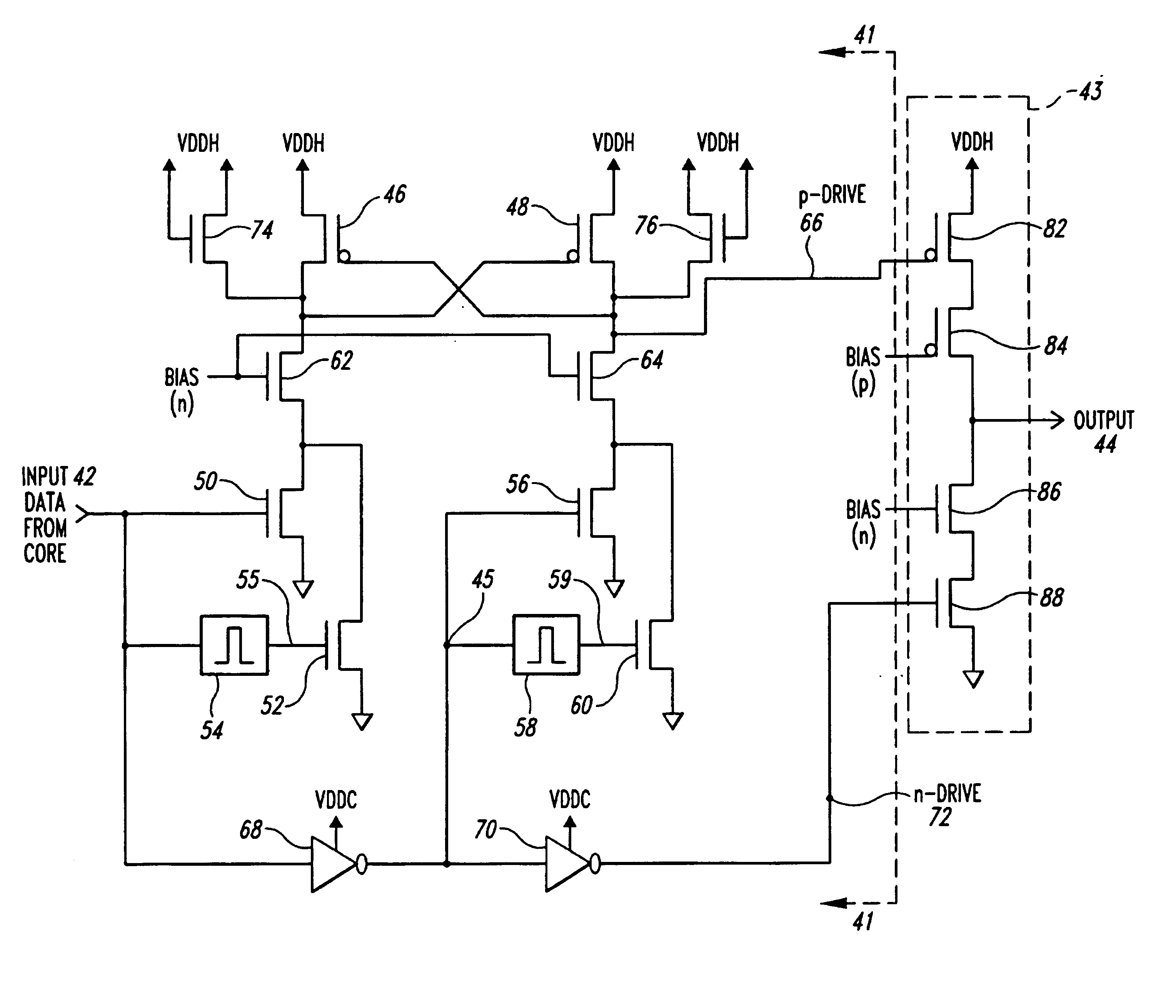
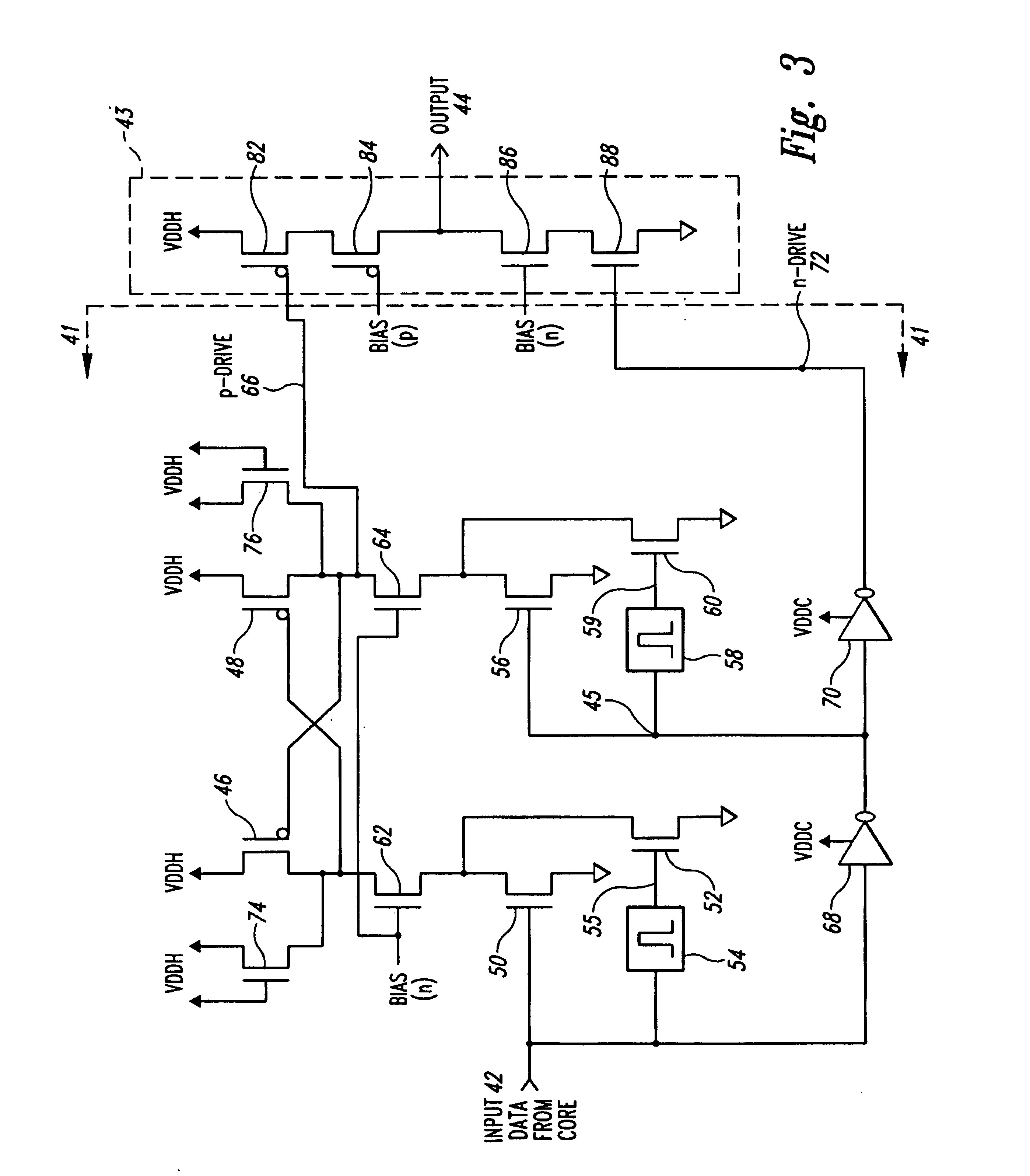
[0014]According to another broad aspect of an embodiment of the invention, disclosed herein is an integrated circuit comprising a core portion including a plurality of transistors made using a first process technology and a level shifting circuit, wherein said level shifting portion includes transistors made only using the first process technology. In one embodiment, the plurality of transistors includes low voltage transistors or transistors having gate oxide layers having low breakdown voltages. A pulse generating circuit may be included for momentarily activating a portion of the transistors of the level shifting circuit, thereby reducing the amount of power consumed by the level shifting circuit. Further, a cascode circuit may be provided for receiving an output of the level shifting circuit.

Problems solved by technology

However, as recognized by the present inventor, forming an integrated circuit through the use of dual gate IC processes increases the complexity and cost of the integrated circuit design.
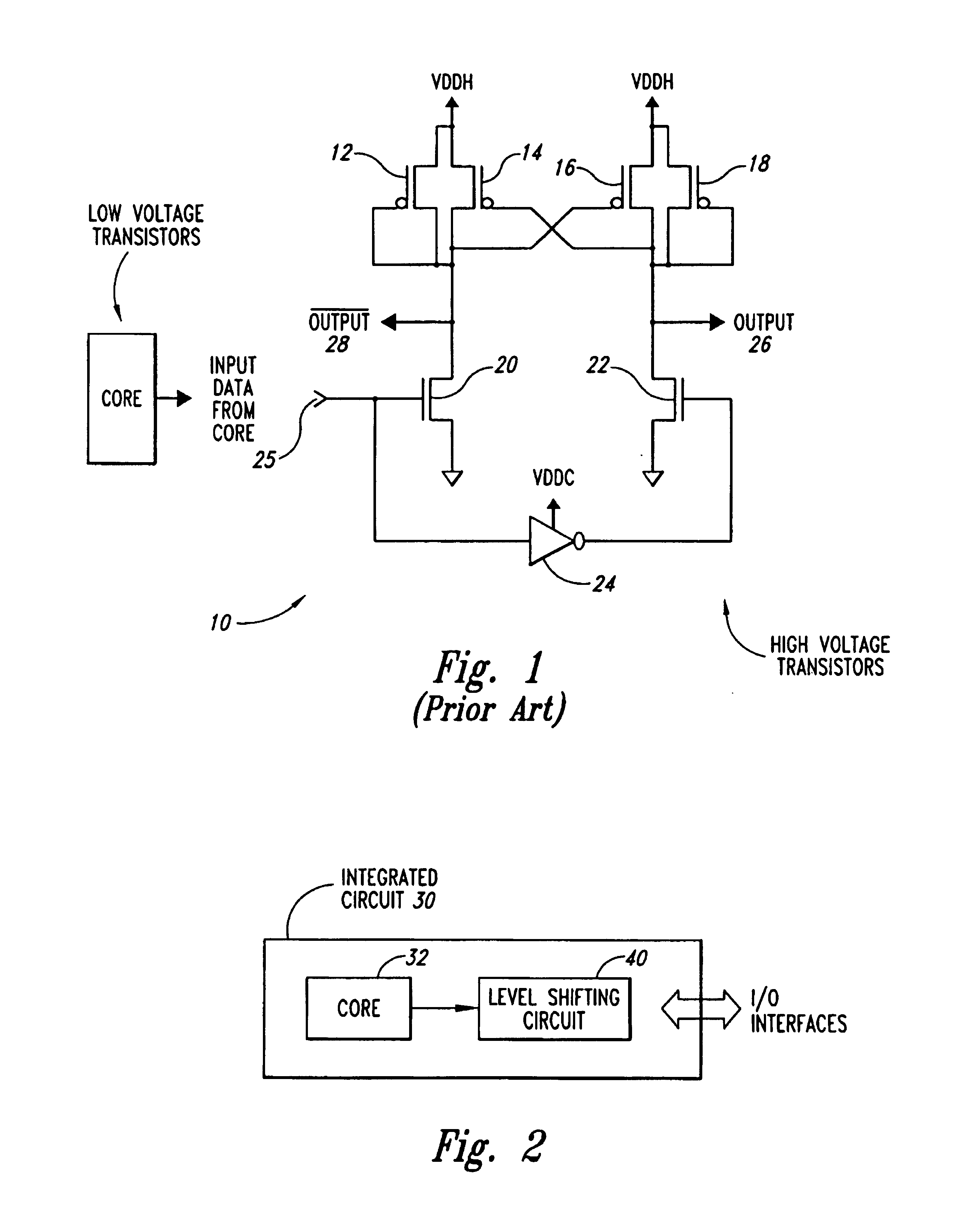
Further, the circuit 10 of FIG. 1 draws standby current even when the circuit is not translating or switching, and general reductions in the standby current have a tendency to slow down the operation of the translating circuit, which is undesirable for high performance, low power applications.
Furthermore, as recognized by the present inventor, in dual gate integrated circuit processes, there may be a tradeoff between the long term reliability of the voltage translating circuit and the speed of the switching of the translating circuit because larger signal swings are desirable for faster translation speeds; however, such larger signals swings may degrade the long term reliability of the device by imposing an unacceptably high level of voltage stress on switching elements of the translating circuit.

Method used


Image

  • Voltage translator circuit formed using low voltage transistors
  • Voltage translator circuit formed using low voltage transistors
  • Voltage translator circuit formed using low voltage transistors

Examples


Embodiment Construction

[0022]FIG. 2 illustrates an integrated circuit 30 having a core 32 and a voltage translating or level shifting circuit 40, in accordance with an embodiment of the present invention. Preferably, the core 32 of integrated circuit 30 may include memory, logic, programmable logic, microprocessors or microcontrollers or portions thereof, timing or clock portions or other circuit or functional blocks therein. In order to reduce the power dissipation of the core, the circuits or elements of the core are made using low voltage transistors or switching elements. Low voltage transistors include, for example, transistors having a gate oxide with a lower breakdown voltage (i.e., a thinner gate) that the other transistors, such as high voltage transistors, which have a higher breakdown voltage (i.e., a thicker gate) and which may dissipate greater amounts of power during normal operation. Lower voltage transistors have characteristics such as low power consumption when compared with other transi...


PUM


Abstract

A circuit for use in conjunction with a portion of a core of an integrated circuit, for shifting a signal from a first voltage level to a second voltage level, wherein the circuit is formed using the same process type transistors (i.e., low voltage transistors) as are used in the core of the integrated circuit.

Description

FIELD OF THE INVENTION[0001]This invention relates to level shifting or voltage translating circuits.BACKGROUND OF THE INVENTION[0002]In the design of integrated circuits, the voltages representative of logic signals at the core of the integrated circuit are often lower than the voltage levels associated with logic signals used by input / output (I / O) sections of the integrated circuit or devices external to the integrated circuit. Accordingly, level shifting circuits or voltage translating circuits are used to shift or translate voltage signals representative of logic levels or data at the core of the integrated circuit to higher voltage levels representative of the same data for use with I / O circuit sections or output devices.[0003]For instance, microprocessors, programmable logic devices, memory devices, timing and clock devices or circuits, all contain I / O interfaces which operate at different voltage levels than the core of the respective integrated circuit. In one example, a cor...

Claims


Application Information

Patent Timeline
Patent Type & Authority Patents(United States)
IPC IPC(8): H03L5/00
CPCH03K19/018521H03K19/0013
Inventor KWONG, DAVID
Owner MONTEREY RES LLC
Learn More