Current difference divider circuit

a current difference and circuit technology, applied in pulse generators, pulse techniques, instruments, etc., can solve the problems of increasing the upper limit value of a read voltage, the inability to read data at high speeds, and the above problem becoming more serious

Inactive Publication Date: 2006-07-04
KK TOSHIBA
View PDF18 Cites 23 Cited by
  • Summary
  • Abstract
  • Description
  • Claims
  • Application Information

AI Technical Summary

Problems solved by technology

This makes it impossible to read data at high speeds.
The above problem becomes more serious in the case of multiple-value data storage architectures with the capability for storing multiple bits of information on a single memory cell transistor, also known as “multiple-bit-level-per-cell” or “multi-level cell (MLC)” technologies.
Unfortunately, such margin expansion in this way can result in an extra increase in the upper limit value of a read voltage(s).
This upper-limit value increase causes application of a higher voltage to memory cells once at a time whenever a read operation is executed, which in turn causes EEPROMs to decrease in reliability.
Another problem encountered with the approach is a decrease in on-chip net areas for layout of memory cells and associative circuitry.
This is resulted from an unwanted increase in chip occupation area of “booster” circuits that are operable to generate any required high potential voltages such as read voltages or else.

Method used


Image

  • Current difference divider circuit
  • Current difference divider circuit
  • Current difference divider circuit

Examples


first embodiment

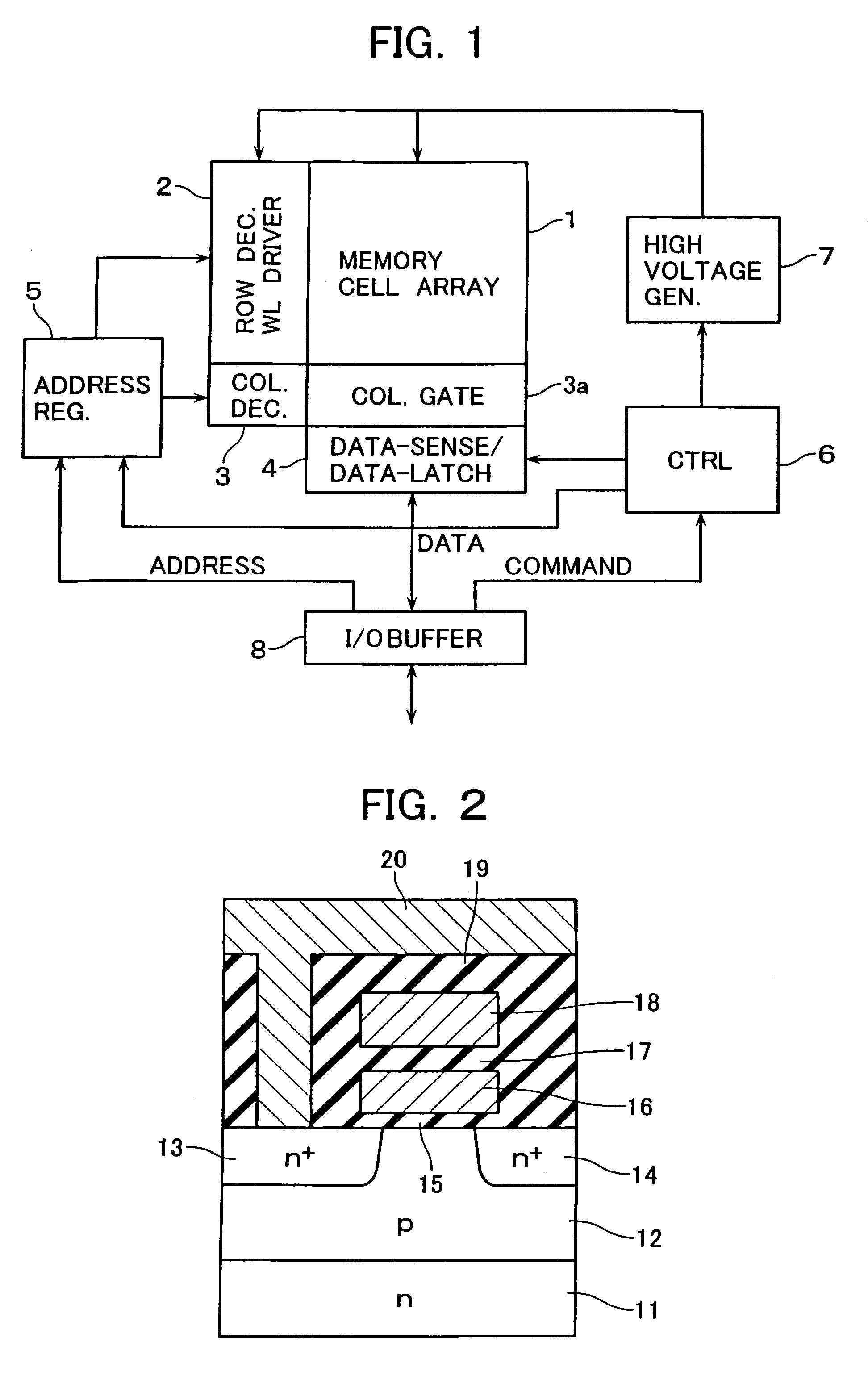
[0035]Referring to FIG. 1, there is shown an overall configuration of an electrically erasable programmable read only memory (EEPROM) device in accordance with one embodiment of this invention. The EEPROM shown herein includes an array 1 of rows and columns of memory cells, which are laid out in a matrix form. This memory cell array 1 may be designed so that its arrangement is of any available types including, but not limited to, the NAND type, NOR type, and DINOR type.

[0036]A single memory cell of the cell array 1 is structured as shown in FIG. 2. An n-type silicon substrate 11 has a surface region for formation of the memory cell array 1, in which region a p-type well 12 is formed. Over this p-type well 12, a floating gate 16 is formed with a tunnel current-flowable gate insulation film 15 which is interposed between p-well 12 and floating gate 16. A control gate 18 is insulatively stacked or “multilayered” over the floating gate 16 with an interlayer dielectric film 17 laid there...

second embodiment

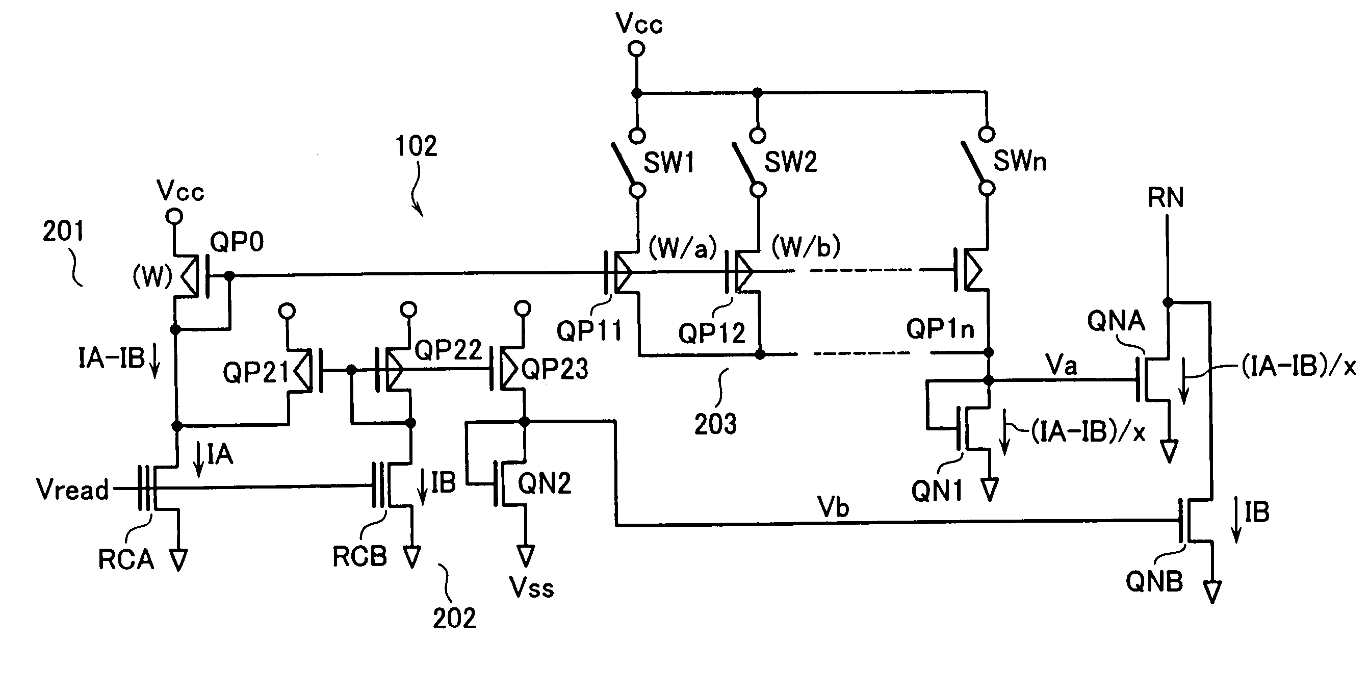
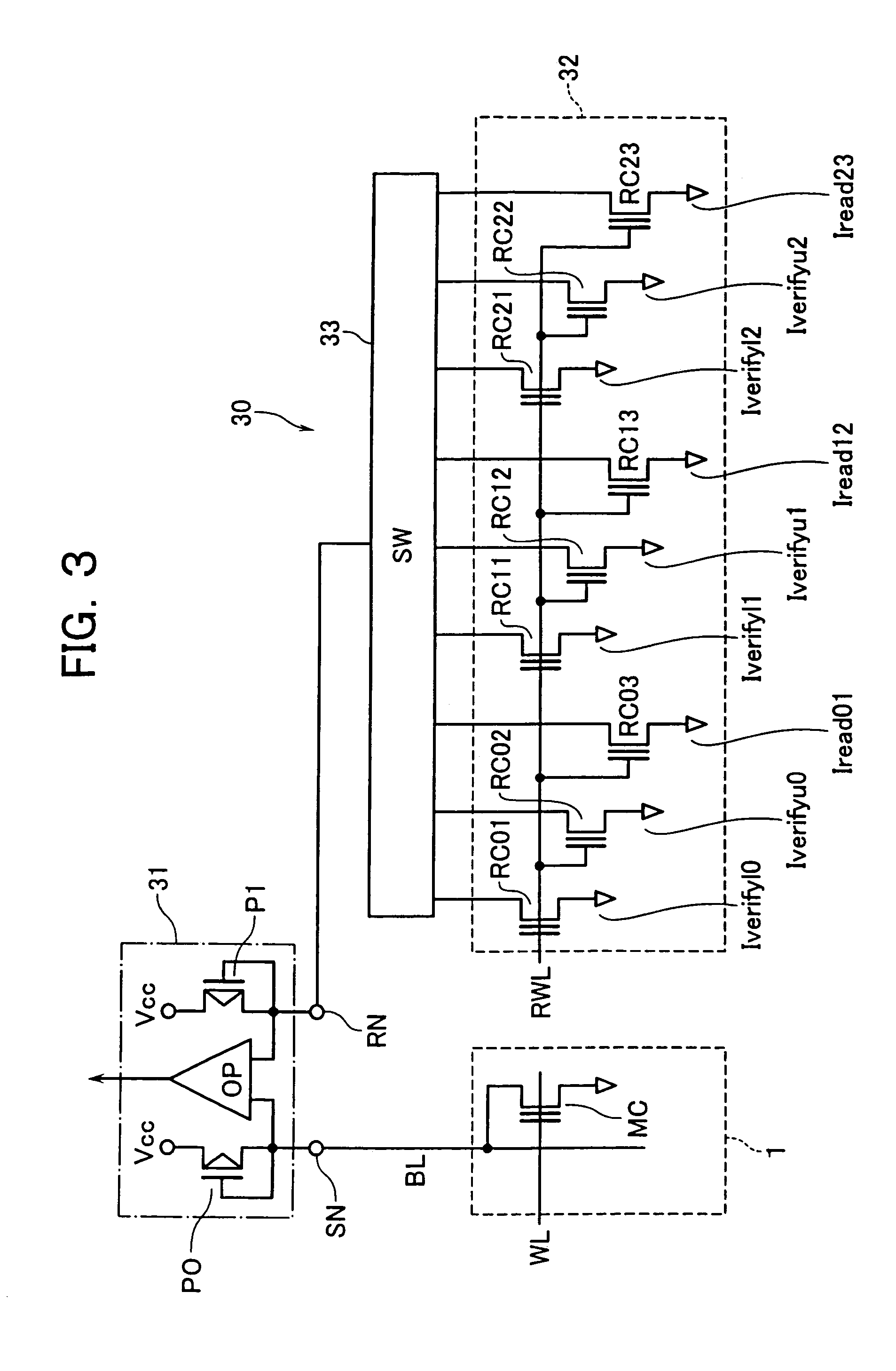
[0062]In FIG. 4, several reference cells RC similar in structure to the memory cells MC are prepared for use as the reference current sources 32 in a way corresponding to the requisite number of reference current values concerned. This approach is modifiable so that a single “basic” reference cell RC is prepared while arranging the reference current source circuit to produce a plurality of other reference currents based on this single reference cell. FIG. 8 shows, in a way corresponding to that of FIG. 3, a configuration of a second embodiment having a reference current source circuit 71 with such an arrangement.

[0063]The reference current source circuit 71 of this embodiment is designed to employ a single reference cell RC0 which conducts a reference current I0 upon application of a read voltage Vread to the control gate thereof. And a division converter circuit 72 is provided for production of a plurality of reference currents I0 / a, I0 / b, . . . , which are subdivided from the refe...

third embodiment

[0070]The second embodiment discussed above is such that the reference cell consists of a single cell RC0, whose reference current is divided into current components or “segments” for production of a plurality of reference currents required. Due to this, simple current division can result in lack of guarantee of the minimal reference current value Iread23 as has been explained in conjunction with FIG. 4. The minimum value of reference current Iread23 is not a mere read-use reference current but the one that offers a capability to guarantee the availability of the minimum read current of a cell. The reason for this is as follows. For instance, in the case of NOR type Flash EEPROMs with an increased number of memory cells being parallel-connected to each bit line, leakage currents of multiple non-selected cells can overlap or “superpose” the current of a selected cell. Thus, any accurate data determination is no longer executable in the state that the current of on-cell is less than a...


PUM


Abstract

A current difference divider circuit with a plurality of current sources is provided. The divider circuit includes a first current source which is operable to generate a first current, a second current source for generation of a second current less in magnitude than the first current, and a third current source for generating a difference current with its magnitude equivalent to a difference between the first and second currents and for generating a third current resulting from the division thereof. The circuit further includes a fourth current source for generating a fourth current obtainable by mirroring of the second current. The third and fourth currents are added together to provide a fifth current, which is then output.

Description

CROSS-REFERENCE TO RELATED APPLICATIONS[0001]This application is a Continuation in Part of U.S. patent application Ser. No. 10 / 661,571, filed Sep. 15, 2003, now U.S. Pat. No. 6,807,097, which is a Divisional of U.S. patent application Ser. No. 10 / 006,395, filed Dec. 10, 2001, now U.S. Pat. No. 6,639,837, issued Oct. 28, 2003, and is based on and claims the benefit of priority from the prior Japanese Patent Application No. 2000-376501, filed on Dec. 11, 2000. The entire contents of these applications are incorporated herein by reference.BACKGROUND OF THE INVENTION[0002]1. Field of the Invention[0003]The present invention relates to current difference dividing circuitry using a plurality of current sources.[0004]2. Description of the Related Art[0005]Electrically erasable programmable read only memories (EEPROMs) are arranged to include an array of memory cells, each of which typically has a transistor structure with a floating gate for electrical carrier retention and a control gate ...

Claims


Application Information

Patent Timeline
Patent Type & Authority Patents(United States)
IPC IPC(8): G05F1/10G11C11/56G11C16/28G11C16/34
CPCG11C11/5621G11C11/5642G11C16/28G11C16/3472G11C16/3481G11C16/3436G11C2211/5634
Inventor TAKANO, YOSHINORITAURA, TADAYUKITANZAWA, TORU
Owner KK TOSHIBA
Why Eureka
Try Eureka