Solid-state imaging device and method of manufacturing said solid-state imaging device

a solid-state imaging and imaging device technology, applied in the direction of semiconductor devices, radio frequency controlled devices, electrical devices, etc., can solve the problems of increasing the size of the whole device, requiring a great deal of mounting time, so as to facilitate manufacturing, facilitate formation, and high reliability

Inactive Publication Date: 2006-07-11
FUJIFILM CORP
View PDF13 Cites 40 Cited by
  • Summary
  • Abstract
  • Description
  • Claims
  • Application Information

AI Technical Summary

Benefits of technology

[0090]According to such a structure, the first semiconductor substrate mounting the IT-CCD thereon and the second semiconductor substrate mounting the peripheral circuit thereon are positioned on a wafer level with respect to the translucent member, and are collectively mounted and integrated, and are thus isolated for each solid-state imaging device. Consequently, it is possible to form a solid-state imaging device which can easily be manufactured and has a high reliability.
[0091]It is desirable that at the semiconductor substrate bonding step, the first and second semiconductor substrates should be bonded to each other by direct bonding. Thus, it is possible to easily carry out the formation without making the substrate dirty due to the protrusion of an adhesive.
[0092]At the semiconductor substrate bonding step, moreover, the first and second semiconductor substrates may be bonded to each other with an adhesive layer in between, and they can easily be bonded to each other without a shift by a photo-curing adhesive layer, a thermosetting adhesive layer or their combination.

Problems solved by technology

Thus, there is a problem in that a great deal of time is required for the mounting because of a large man-hour.
Thus, there is a problem in that a great deal of time is required for the mounting because a large number of components are provided.
Moreover, there has been a serious problem in that various peripheral circuits are necessary with a requirement for an enhancement in a resolution, resulting in an increase in the size of the whole device.

Method used


Image

  • Solid-state imaging device and method of manufacturing said solid-state imaging device
  • Solid-state imaging device and method of manufacturing said solid-state imaging device
  • Solid-state imaging device and method of manufacturing said solid-state imaging device

Examples


tenth embodiment

[0311]Next, a tenth embodiment of the invention will be described.

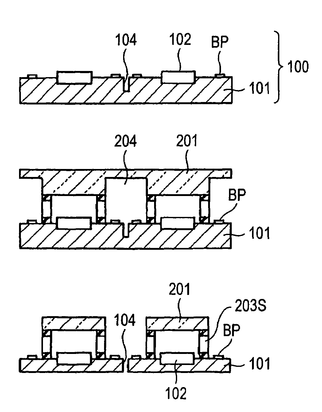
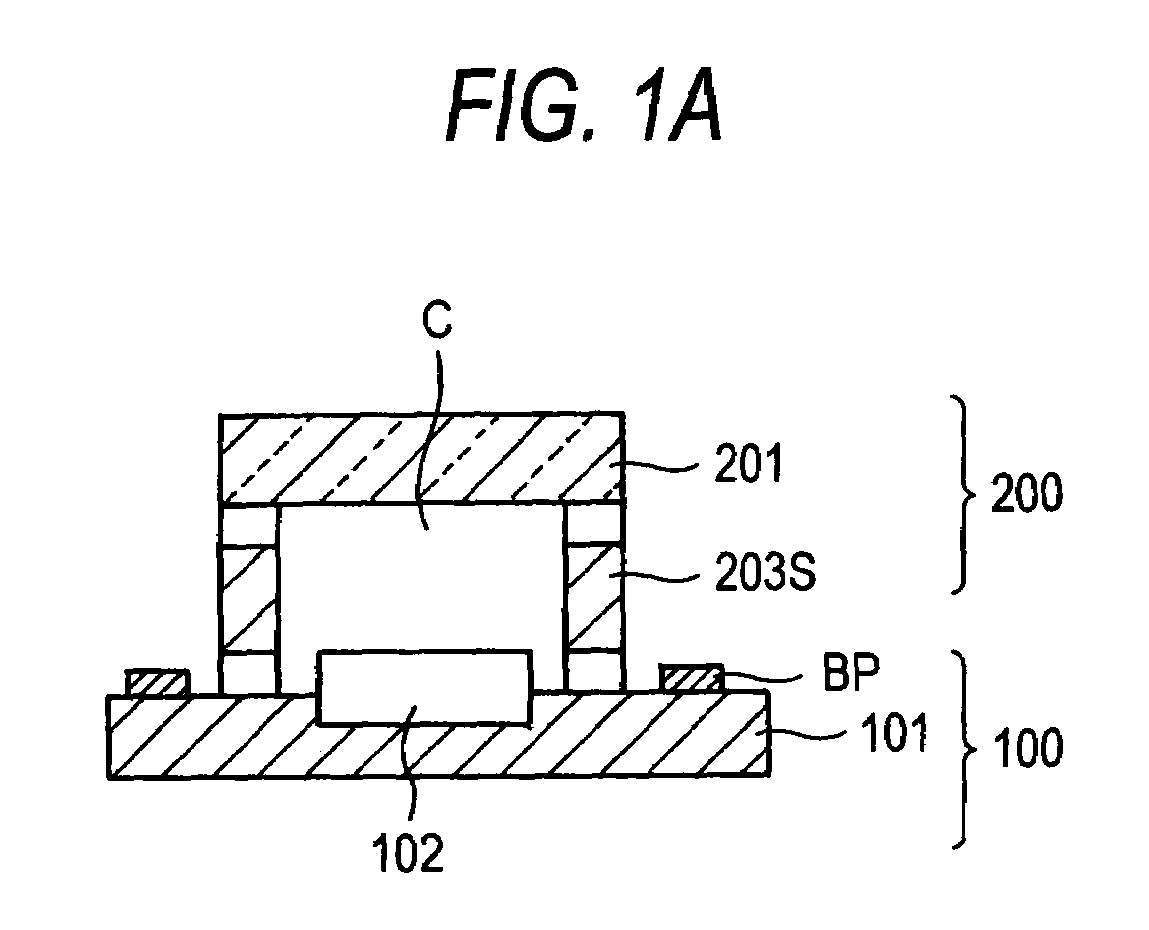
[0312]In the first to ninth embodiments, the silicon substrate 203 to be a spacer is stuck to the glass substrate 201 through an adhesive, and the silicon substrate 203 is subjected to the patterning to form the cut trench 204 by an etching method using photolithography in the formation of the sealing cover glass 200 provided with the spacer 203S as shown in FIGS. 2A and 2B. In the embodiment, as shown in FIGS. 12A and 12B, the spacer 203S is etched over a dummy plate by using a dummy plate 501 and sticking to the glass substrate 201 is then carried out with an adhesive layer 202. Other portions are formed in the same manner as those in the embodiments.

[0313]More specifically, as shown in FIG. 12A, the silicon substrate 203 to be the spacer is stuck to the dummy plate 501 formed by a silicon substrate through an adhesive layer 502 having a softening temperature of approximately 50 to 150 degree C. Then, the silicon su...

eleventh embodiment

[0320]Next, an eleventh embodiment of the invention will be described.

[0321]While the spacer 203S is separately formed and is stuck through the adhesive layer in the first to tenth embodiments, a concave portion 205 is formed and a spacer 206 is thus provided on a glass substrate 201 by an etching method using photolithography in this example. Other portions are formed in the same manner as those in the embodiments.

[0322]More specifically, as shown in FIG. 14A, the glass substrate 201 is prepared.

[0323]As shown in FIG. 14B, then, the concave portion 205 is formed by the etching method using the photolithography. Consequently, a glass substrate comprising the spacer 206 is formed.

[0324]According to such a structure, the spacer 206 is integrally formed. Therefore, manufacture can easily be carried out and a shift is not generated, and furthermore, there is no possibility that a strain might be generated in a bonded portion.

twelfth embodiment

[0325]Next, a twelfth embodiment of the invention will be described.

[0326]While the description has been given to the method of forming the sealing cover glass 200 having the spacer 206 formed integrally therewith in the eleventh embodiment, it is also possible to form a trench section 204 by etching as shown in FIGS. 15A to 15C.

[0327]In this example, a concave portion 205 is formed on a glass substrate 201 by an etching method using photolithography so that the spacer 206 is formed integrally. Then, the trench section 204 is formed. Consequently, the trench section 204 of the glass substrate for positioning the edge of the sealing cover glass 200 on the inside of the edge of an IT-CCD substrate 100 is formed by the etching. Accordingly, the generation of a strain is reduced and the isolating step can be thereby carried out easily.

[0328]More specifically, as shown in FIG. 15A, the glass substrate 201 is prepared.

[0329]As shown in FIG. 15B, then, the concave portion 205 is formed on ...


PUM


Abstract

It is an object to provide solid-state imaging device, which can easily be manufactured and has a high reliability, and a method of manufacturing the solid-state imaging device. In the present invention, a manufacturing method comprises the steps of forming a plurality of IT-CCDs on a surface of a semiconductor substrate, bonding a translucent member to the surface of the semiconductor substrate in order to have a gap opposite to each light receiving region of the IT-CCD, and isolating a bonded member obtained at the bonding step for each of the IT-CCDs.

Description

[0001]This application is a continuation-in-part of application Ser. No. 10 / 419,861 filed on Apr. 22, 2003, now abandoned, the entire contents of which are hereby incorporated by reference and for which priority is claimed under 35 U.S.C. § 120.[0002]This application also claims priority under 35 USC 119 on 2002-119262, 2002-154528, 2002-183072, 2002-219645 and 2002-219791 filed in Japan on Apr. 22, 2002, May 28, 2002, Jun. 24, 2002, Jul. 29, 2002 and Jul. 29, 2002, respectively.BACKGROUND OF THE INVENTION[0003]1. Field of the Invention[0004]The present invention relates to a solid-state imaging device and a method of manufacturing the solid-state imaging device. More particularly, the invention relates to a solid-state imaging device of a chip size package (CSP) type in which a microlens is integrally provided on a chip.[0005]2. Description of the Related Art[0006]A reduction in the size of a solid-state image pickup device, such as a CCD (Charge Coupled Device), has been required ...

Claims


Application Information

Patent Timeline
Patent Type & Authority Patents(United States)
IPC IPC(8): H01L21/00H01L27/148
CPCH01L27/14618H01L27/14625H01L27/14632H01L27/14636H01L27/14687H01L27/148H01L27/14806H01L2924/01322H01L2224/4847H01L2924/01078H01L2924/01079H01L2924/09701H01L2924/3025
Inventor MAEDA, HIROSHINISHIDA, KAZUHIRONEGISHI, YOSHIHISAHOSAKA, SHUNICHI
Owner FUJIFILM CORP
Why Eureka
Try Eureka