Method for distributing clock signals to flip-flop circuits

Inactive Publication Date: 2006-07-11
KK TOSHIBA
View PDF54 Cites 17 Cited by
  • Summary
  • Abstract
  • Description
  • Claims
  • Application Information

AI Technical Summary

Benefits of technology

[0023]According to a first aspect of the present invention, a method for distributing clocks to flip-flop circuits which constitute a logic circuit includes obtaining a timing slack of a first minimum delay time with respect to a minimum delay constraint time and a timing slack of a first maximum delay time with respect to a maximum delay constraint time for a clock in an input path to a flip-flop circuit, obtaining a timing slack of a

Problems solved by technology

One problem, which arises quite often in designing digital logic integrated circuits, is that this skew becomes so large that the synchronization operation of circuits cannot be performed at a desired clock frequency.
Moreover, in the case of zero skew, if even one flip-flop circuit of the logic circuit does not satisfy a predetermined requirement, the entirety of circuit does not work well.
However, the use of useful skew makes it possible to operate a flip-flop circuit which does not require the predetermined requirement in the case of zero skew properly, and to avoid a problem in which the entirety of circuit does not work well.
Accordingly, this method does not fully bring out the merit of using the useful skew.
However, there is no description about an algorithm such as a point that the skew value is aggressively set to a value away from the center of the skew boundary, thereby reducing the peak current value positively.
Moreover, in addition to the forego

Method used


Image

  • Method for distributing clock signals to flip-flop circuits
  • Method for distributing clock signals to flip-flop circuits
  • Method for distributing clock signals to flip-flop circuits

Examples


first embodiment

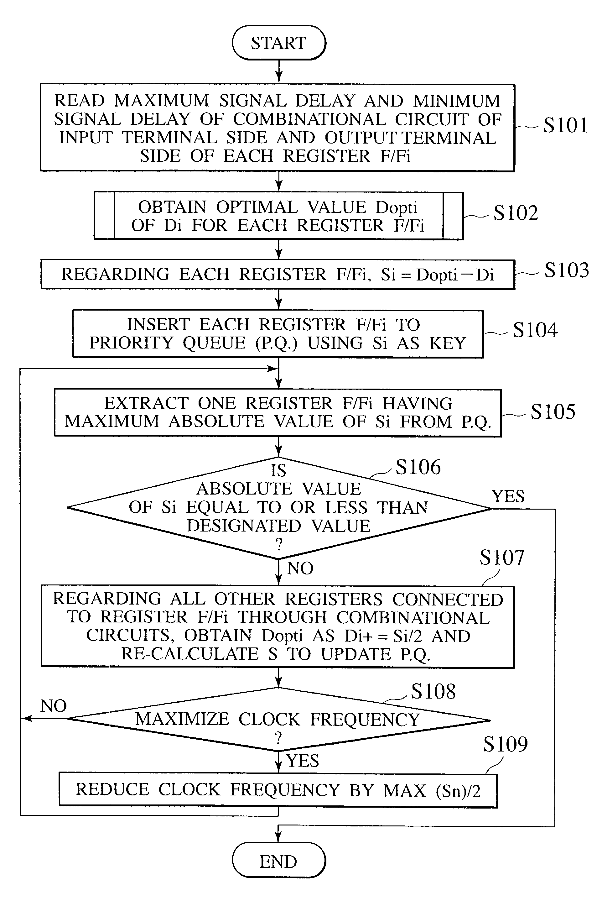
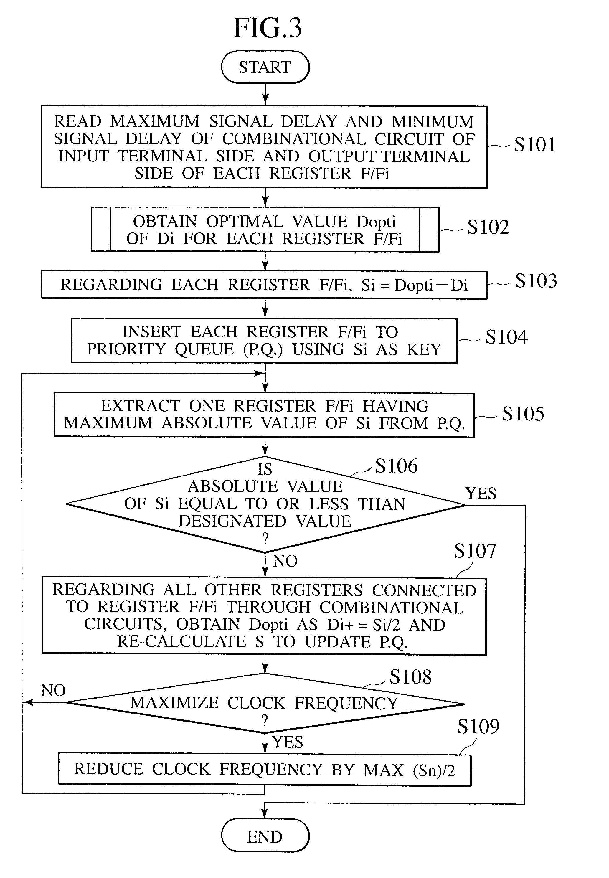
[0053]A clock distributing method according to a first embodiment of the present invention will be explained with reference to the flowchart of FIG. 3 and the block diagram of FIG. 4. First, a circuit shown in FIG. 4 includes a flip-flop circuit F / Fi (hereinafter simply referred to as F / Fi or F / Fi circuit) 11i that receives an input signal from an external input terminal 10 and a clock signal from a CLK terminal 14, a first combinational circuit 12a that receives an output from the F / Fi circuit 11i, an F / Fj circuit 11j that receives an output from the first combinational circuit 12a and a clock signal from the CLK terminal 14, a second combinational circuit 12b that receives an output from the F / Fj circuit 11j, an F / Fk circuit 11k that receives an output from the second combinational circuit 12b and a clock signal from the CLK terminal 14, and an external output terminal 13 that finally outputs a signal from the F / Fk circuit 11k. Here, it is assumed that the delay time of the clock ...

second embodiment

[0096]The processes in steps of a second embodiment shown by a flowchart of FIG. 6 are substantially the same as those of the first embodiment shown by FIG. 3. However, to obtain a useful skew, it is necessary to add signal delay information of the combinational circuit between the flip-flop circuits F / F, so that the number of combinational circuits becomes considerably large, resulting in an increase in memory amounts and processing time used.

[0097]In order to prevent the above problem, step S401 is performed in the following manner, which is different from the first embodiment, based on the idea that a correct useful skew can be obtained even if the amount of signal delay time information of the combinational circuit is limited.

[0098]Specifically, regarding signal delay time, it is generally necessary to add two kinds including maximum time and minimum time. However, in the second embodiment, (100−n) % of clock cycle Tcp, for example, only information of maximum times over 80% and...

third embodiment

[0107]The processes in steps of a third embodiment shown by a flowchart of FIG. 8 are substantially the same as those of the first embodiment shown in FIG. 3. However, this embodiment is different from the first embodiment in the aspect that high priority is given to either reduction of a setup time constraint violation or that of a hold time constraint violation to obtain an optimal value Dopti at the time of obtaining a useful skew in step S602. The priority is given by the user's designation to either the setup time constraint violation or the hold time constraint violation. In this case, regarding each flip-flop circuit F / Fi, at the time of obtaining Di from a value based on the setup time constraint and that based on the hold time constraint, there is provided a means for deciding Di preferentially to prevent the occurrence of violation in either of these constraints in accordance with the user's designation necessarily.

[0108]FIG. 9 is a sub-routine in step S602. In step S6021,...


PUM


Abstract

A method for distributing clocks to flip-flop circuits which constitute a logic circuit includes obtaining a timing slack of a first minimum delay time with respect to a minimum delay constraint time and a timing slack of a first maximum delay time with respect to a maximum delay constraint time for a clock in an input path to a flip-flop circuit, obtaining a timing slack of a second minimum delay time with respect to a minimum delay constraint time and a timing slack of a second maximum delay time with respect to a maximum delay constraint time for a clock in an output path from all the flip-flop circuits which receive the clocks from a clock terminal directly and obtaining a delay value which maximizes a minimum value of each of the first and second minimum delay time and maximum delay time of timing slacks.

Description

CROSS REFERENCE TO RELATED APPLICATIONS[0001]This application is based upon and claims the benefit of priority from the prior Japanese Patent Application No. P2001-202579, filed on Jul. 3, 2001; the entire contents of which are incorporated herein by reference.BACKGROUND OF THE INVENTION[0002]1. Field of the Invention[0003]The present invention relates to a clock distribution method for setting an optimal skew of a logic circuit, which obtains an optimal skew between registers on an LSI clock tree circuitry, a clock tree generating method to structure a clock tree when a useful skew is used, a clock delay setting method to minimize noise generated by a circuit, and a circuitry process method for a logic circuit using a useful skew.[0004]2. Description of the Related Art[0005]Conventionally, in digital logic integrated circuits, sequential circuits, typically registers and flip-flop circuits, are used, and the entire of the circuit operates in synchronization with a plurality of cloc...

Claims


Application Information

Patent Timeline
IPC IPC(8): H03K19/00G06F1/12G06F17/50G06F9/45H03K19/096G06F1/10H01L21/82
CPCG06F17/5045G06F1/10G06F30/30
Inventor KOJIMA, NAOHITOMINAMI, FUMIHIROMURAKATA, MASAMIISHIOKA, TAKASHI
Owner KK TOSHIBA
Why Eureka
Try Eureka