Microelectronic packages with elongated solder interconnections

a technology of microelectronic packages and interconnections, which is applied in the direction of printed circuit aspects, sustainable manufacturing/processing, final product manufacturing, etc., can solve the problems of thermal fatigue stress on the solder bond in such assemblies, temperature rise and fall of the assembly, temperature rise and fall of the chip and circuit panel, etc., to achieve enhanced flexibility and fatigue resistance, the effect of relieving the stress on the bond

Inactive Publication Date: 2006-07-18
TESSERA INC
View PDF34 Cites 19 Cited by
  • Summary
  • Abstract
  • Description
  • Claims
  • Application Information

AI Technical Summary

Benefits of technology

[0010]In a particularly preferred method according to this aspect of the invention, the first element includes a dielectric packaging structure having an interior surface facing toward the second element and having an exterior surface. The pads of the first element are disposed on the interior surface. The packaging structure further includes terminals exposed at the exterior surface which are electrically connected to the pads on the interior surface. Desirably, the second element includes one semiconductor chip or a plurality of semiconductor chips. Preferred methods according to these embodiments of the invention, thus can provide packaged microelectronic elements, such as packaged semiconductor chips, incorporating the microelectronic element and an interposer having terminals connected to the microelectronic element by elongated solder columns. Such an assembly can be utilized by bonding the terminals of the interposer to a circuit panel or other substrate. The assembly can be handled and mounted using standard techniques. The elongated solder columns provide enhanced resistance to stress as compared to standard flip-chip mountings, but without the need for special techniques during assembly of the chip to the circuit panel.
[0011]Methods according to this aspect of the invention desirably include the step of injecting a liquid material around the solder masses and curing the liquid to form dielectric encapsulant, desirably a compliant encapsulant, surrounding the elongated solder columns. For example, the fluid used to force the elements away from one another may be a liquid, uncured encapsulant. Where the second element includes a plurality of chips, the method may include the step of separating the chips from one another after the step of moving the elements away from one another, and desirably after cooling the solder masses to below their solidus temperature. The dielectric packaging structure or interposer may be severed in this separating step. The separating step forms a plurality of unit assemblies, each of which includes one or more of the chips and a portion of the packaging structure or interposer associated with such chip or chips. For example, the method may be performed at a wafer level, with a large interposer covering the entire wafer. The interposer and the wafer may be severed to provide unit assemblies. The first element used in the process may include a reinforcing element engaged with the first element. This approach is particularly useful where the first element is a flexible dielectric element such as a packaging structure. For example, the packaging structure may be held taut on a frame extending around the periphery of the packaging structure. Alternatively or additionally, the reinforcing element may extend along the exterior of the packaging structure. The method desired further includes the steps of at least partially removing the reinforcing structure after the moving step. The reinforcing structure holds the pads of the packaging structure precisely in position and facilitates registration of the packaging structure with the pads of the microelectronic elements. This is particularly useful where the process is performed on a wafer level.
[0012]A further aspect of the present invention provides methods of making solder connections which include the steps of providing first and second elements having confronting surfaces and having pads on the confronting surfaces arranged in pairs, each pair including a pad on one element and a pad on the other element, and providing solder masses at at least some of the pairs so that each such solder mass is in contact with both pads of the pair. Methods according to this aspect of the invention also include the step of moving the elements away from one another through a preselected vertical movement so as to stretch the solder masses while the solder masses are at a temperature above the recrystallization temperature of the solder but below its recrystallization temperature. In methods according to this aspect of the invention, the solder masses incorporate columnar inclusions, which are present when the solder masses are stretched. As used in this disclosure, the term “columnar inclusion” refers to a separate phase within the solder present as elongated droplets or particles. For example, the moving step may be performed at least in part at a temperature between the solidus and liquidus temperatures of the solder masses, and the columnar inclusions may be present as solid inclusions within the partially molten solder masses during the moving step. Such columnar inclusions will be formed, for example, by lead-tin alloy solders containing about one percent to about five percent copper by weight. As the solder masses are stretched during the moving step, the columnar inclusions tend to orient preferentially in the direction of movement, and hence orient along the long axis of the elongated solder masses resulting from the moving step. Columnar inclusions further enhance resistance of the elongated solder masses to fatigue failure.
[0013]A method according to a further aspect of the invention includes the step of providing first and second elements with pairs of pads as aforesaid, and with solder masses at at least some pairs such that each solder mass is in contact with both pads of the associated pad. Methods according to this aspect of the invention include the further step of moving the elements relative to one another, while the solder masses are at a temperature above the recrystallization temperature of the solder, so that the elements move relative to one another in a horizontal direction parallel to the confronting surfaces so as to deform the solder masses in the horizontal direction. Desirably, the method also includes the step of moving the elements away from one another in a vertical direction, transverse to the confronting surfaces while the solder masses are at a temperature above the recrystallization temperature. Most preferably, the vertical and horizontal movements are performed simultaneously. The pads constituting each pair may be aligned one above the other prior to the horizontal movement and may be offset from one another in the horizontal direction after the horizontal movement step. Methods according to this aspect of the invention yield assemblies incorporating elongated solder masses having directions of elongation which are inclined to the confronting surfaces of the components. The sloping, elongated solder masses provide enhanced flexibility in the assembly.
[0015]Yet another aspect of the invention provides packaged microelectronic elements such as semiconductor chips. A packaged microelectronic element according to this aspect of the invention includes a microelectronic element such as a semiconductor chip together with an interposer overlying the contact-bearing surface of the chip. The interposer desirably is a flexible sheetlike element and includes an interior surface facing toward the chip and pads on the interior surface. The interposer further includes terminals exposed for connection to external components. The terminals may be exposed at an exterior surface of the interposer, facing away from the chip. The terminals are electrically connected to the pads over the interposer. The pads of the interposer in turn are electrically connected to the pads of the microelectronic element to a semiconductor chip by elongated solder masses extending between the pads of the interposer and the pads of the micro electronic element chip. Most desirably, the assembly includes a compliant dielectric layer such as a gel, foam or elastomer surrounding the elongated solder masses. Such an assembly can be handled and the amount of using standard surface mounting techniques, as by solder bonding the terminals of the interposer to a circuit panel or other substrate. After assembly, flexure of the elongated solder masses provides compensation for differential thermal expansion, and relieves stress on the bonds between the terminals and the circuit panel.
[0016]Yet another aspect of the invention provides a soldered assembly, such as a packaged microelectronic element or other assembly which includes first and second elements with pairs of pads thereon and which includes solder masses, each such solder mass extending between the pads of one such pair. The solder masses incorporate columnar inclusions. Most preferably, the columnar inclusions in at least some of the solder masses are oriented preferentially in the direction between the pads of the associated pair. That is, the lengthwise direction of the columnar inclusions is preferentially oriented in alignment with the direction between the pads. Yet a further aspect of the invention provides solder assemblies with elongated solder masses extending between pairs of pads on opposing surfaces of two elements. The pads of each pair are spaced apart from one another in a vertical direction normal to the confronting surfaces of the element and are offset from one another in a horizontal direction parallel to the confronting surfaces so that the elongated solder masses extend oblique to the vertical and horizontal directions, and oblique to the surfaces of the opposing elements. Most desirably, the elongated solder masses extend generally parallel to one another. The oblique orientation of the elongated solder masses provides enhanced flexibility and fatigue resistance. Here again, the various aspects of the invention can be combined with one another to form an assembly, such as a packaged chip, which includes all of the features discussed above with reference to the assembly.

Problems solved by technology

The solder bonds in such assemblies typically are subjected to thermal fatigue stress during manufacture and during use of the assembly.
The electrical power dissipated within the chip and other elements of the assembly tends to heat the chip and the circuit panel, so that the temperatures of the chip and circuit panel rise and fall depending on use of the device.
Processing operations during manufacturing also cause the temperature of the assembly to rise and fall.
Differential expansion and contraction causes the contact pads on the chip to move relative to the contact pads on the substrate, which in turn tends to strain the solder bonds.
The barrel-shaped solder bonds resulting from conventional C4 bonding techniques are susceptible to failure under these conditions.
Chip mounting procedures using elongated solder columns heretofore have suffered form considerable drawbacks.
These procedures require specialized techniques and considerable care during mounting of the chip to the circuit panel.
Moreover, these procedures require handling and testing of bare, unpackaged semiconductor chips.
It is difficult to test such a bare chip prior to attachment of the chip to the circuit panel.
Moreover, the bare chip is susceptible to damage during handling and testing.

Method used


Image

  • Microelectronic packages with elongated solder interconnections
  • Microelectronic packages with elongated solder interconnections
  • Microelectronic packages with elongated solder interconnections

Examples


Embodiment Construction

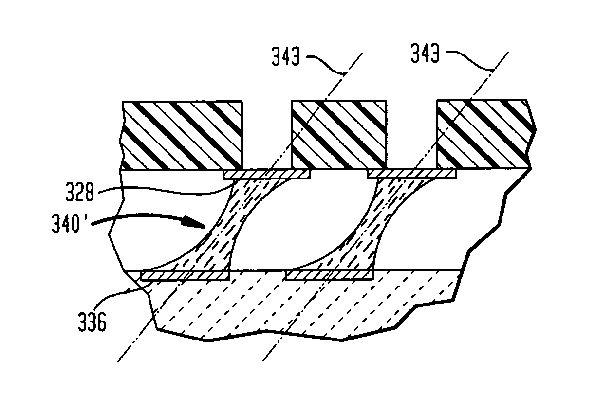
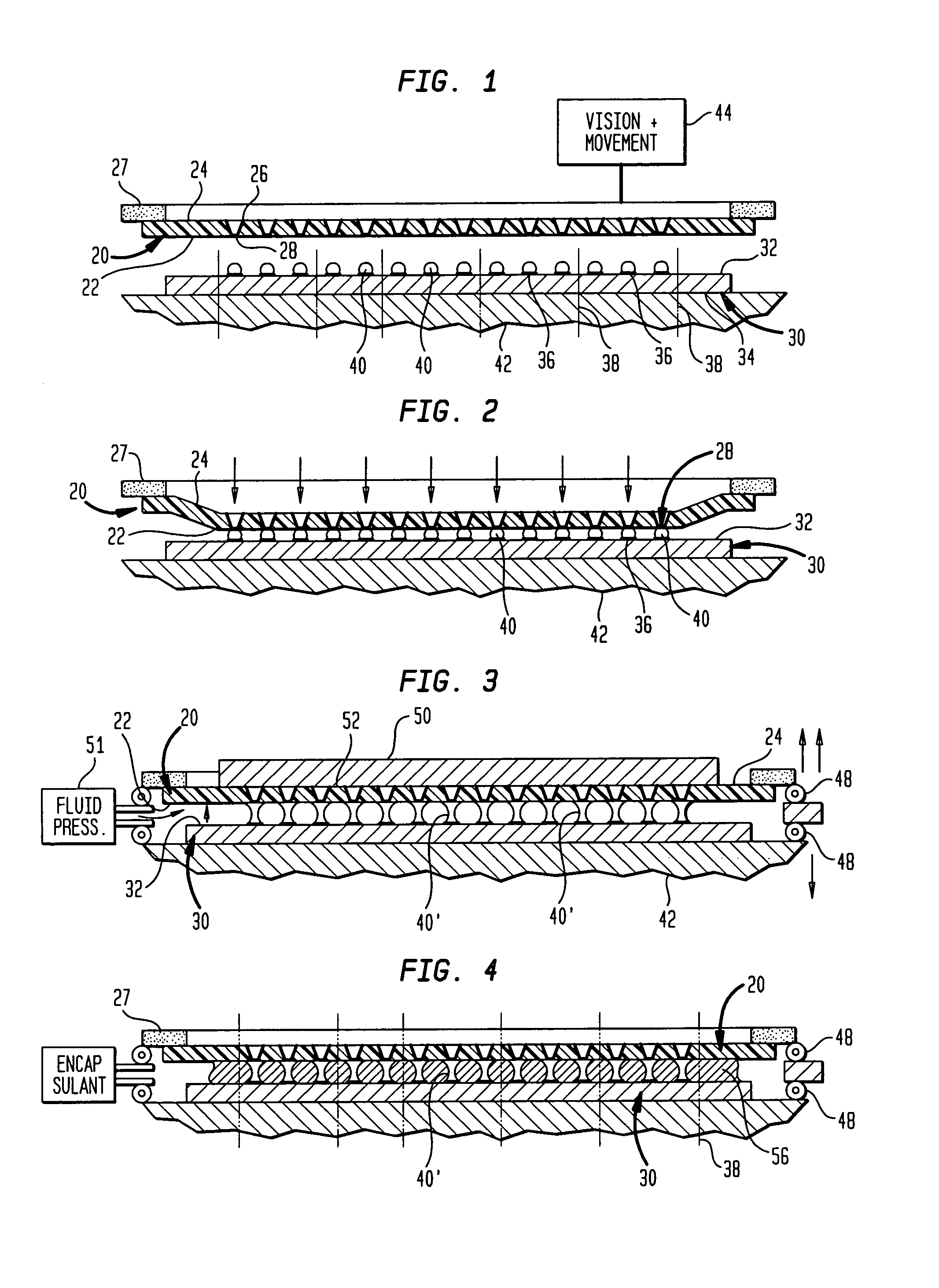
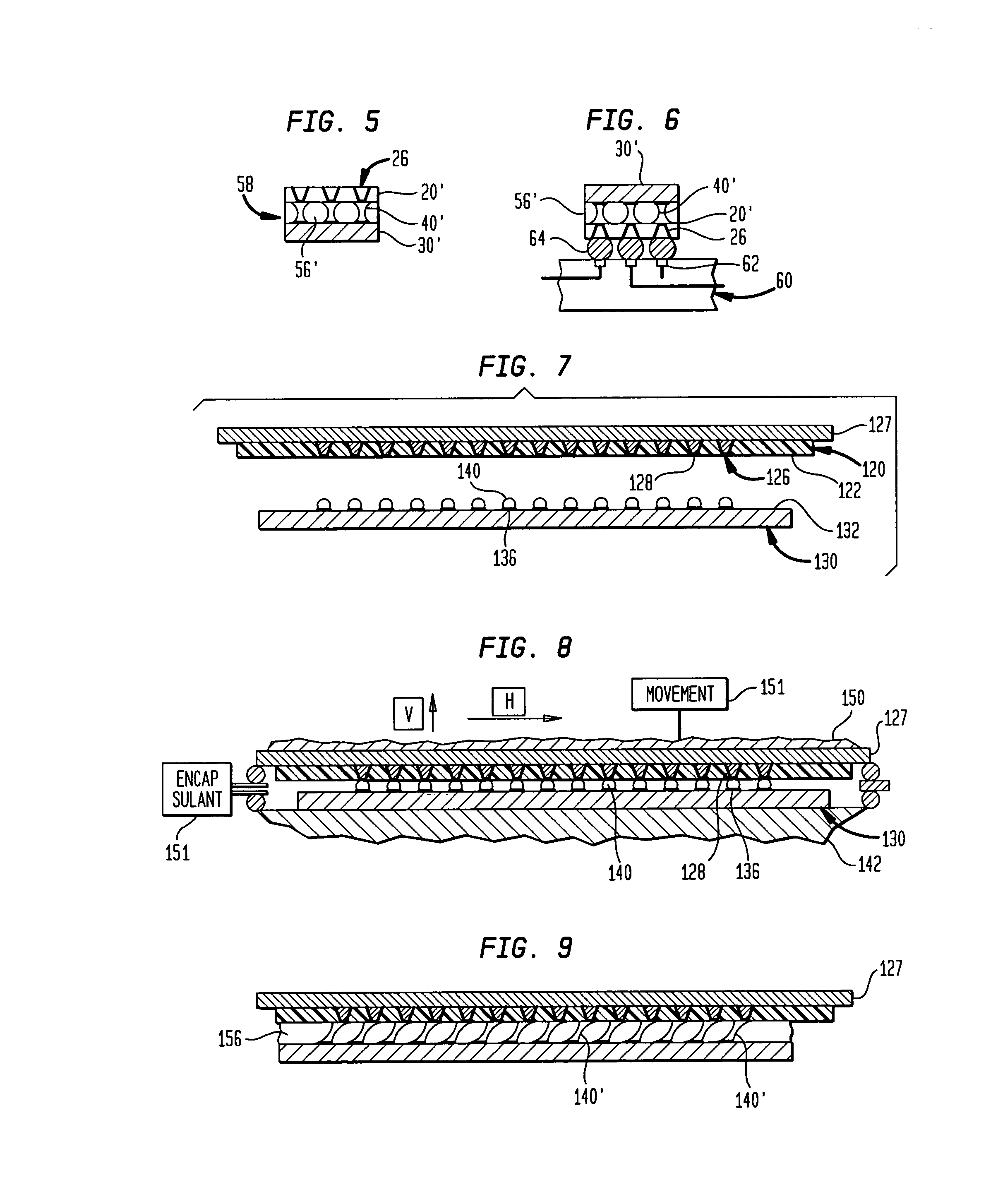
[0026]A process in accordance with one embodiment of the invention utilizes a flexible dielectric sheet 20 having oppositely facing inner surface 22 and outer surface 24. Sheet 20 may be formed from the polymeric materials such as a polyimide. The thickness of sheet 20 is greatly exaggerated in FIG. 1 for clarity of illustration. Typically, sheet 20 is about 25–100 μm thick. Sheet 20 has numerous holes extending through it. These holes are provided with metallic via liners 26. Each via liner defines a pad 28 on the inner surface 22 of the sheet. Each via liner is also exposed at the outer surface 24 of the sheet. Sheet 20 is attached to a ring-like frame 27 formed from a rigid material. The sheet may be stretched on the frame in the manner disclosed in U.S. Pat. No. 5,518,964, the disclosure of which is hereby incorporated by reference herein and in the manner discussed in co-pending, commonly assigned U.S. Provisional Patent Application No. 60 / 061,932 filed Oct. 17, 1997, the discl...


PUM


Abstract

A soldered assembly for a microelectronic element includes a microelectronic element, solder columns extending from a surface of the microelectronic element and terminals connected to distal ends of the columns. The assembly can be handled and mounted using conventional surface-mount techniques, but provides thermal fatigue resistance. The solder columns may be inclined relative to the chip surface, and may contain long, columnar inclusions preferentially oriented along the lengthwise axes of the columns.

Description

CROSS-REFERENCE TO RELATED APPLICATIONS[0001]This is a divisional of U.S. patent application Ser. No. 09 / 157,047, filed Sep. 18, 1998, the disclosure of which is hereby incorporated by reference herein. Said '047 application claims benefit of U.S. Provisional Patent Application 60 / 059,225, filed Sep. 18, 1997, the disclosure of which is hereby incorporated by reference herein.BACKGROUND OF THE INVENTION[0002]Microelectronic elements such as semiconductor chips have been connected to circuit panels by soldering. One technique which has been utilized heretofore is referred to as “flip chip” bonding. In flip chip bonding, the front surface of the chip bearing the contact pads of the chip faces downwardly, towards the surface of a circuit panel having a pattern of pads matching the pattern of the contact pads on the chip. The pads on the chip are bonded to the mating pads on the substrate. In one variant of this technique, referred to as a “controlled collapse chip connection” or “C4” b...

Claims


Application Information

Patent Timeline
Patent Type & Authority Patents(United States)
IPC IPC(8): H01L23/48H01L23/52H01L29/40H01L21/56H01L21/60H05K3/34
CPCH01L21/561H01L21/563H01L21/568H01L21/6835H01L23/49805H01L23/49811H01L24/11H01L24/12H01L24/16H01L24/29H01L24/742H01L24/81H01L24/94H05K3/3436H05K3/363H01L24/27H01L23/3114H01L2224/11003H01L2224/1184H01L2224/131H01L2224/13111H01L2224/274H01L2224/29298H01L2224/73203H01L2224/81801H01L2924/01002H01L2924/01005H01L2924/01013H01L2924/01015H01L2924/01018H01L2924/01027H01L2924/01029H01L2924/01042H01L2924/0105H01L2924/01078H01L2924/01082H01L2924/18301H05K2201/0215H05K2201/0248H05K2201/09427H05K2201/10977H05K2203/0465H05K2203/074H05K2203/306H01L2924/00013H01L2924/01006H01L2924/01023H01L2924/01033H01L2924/014H01L2224/29101H01L2224/02319H01L2224/02333H01L2224/0401H01L2224/13099H01L2924/00H01L2924/3512H01L2224/29099H01L2224/29199H01L2224/29299H01L2224/2929H01L2924/12042Y02P70/50
Inventor DISTEFANO, THOMAS H.
Owner TESSERA INC
Why Eureka
Try Eureka