Memory array with low power bit line precharge

a memory array and low power bit line technology, applied in the field of integrated circuit memory devices, can solve the problems of limiting the size and speed of memory devices, limiting the speed of such sensing systems, and the requirement of complex biasing structures on every bit line, and limiting the size and cost of integrated circuit memory

Active Publication Date: 2006-07-25
MACRONIX INT CO LTD
View PDF9 Cites 26 Cited by
  • Summary
  • Abstract
  • Description
  • Claims
  • Application Information

AI Technical Summary

Benefits of technology

[0011]An integrated circuit memory device is described including an array of memory cells with an extra column of memory cells and a reference bit line coupled to the extra column, in which the reference bit line acts as a reference for a shared clamping control bias on the bit lines in the array. The memory device in an embodiment described herein includes an array of memory cells with a plurality of columns and rows. A plurality of bit lines is coupled to the columns in the array and a plurality of word lines is coupled to the rows in the array. The extra column of memory cells and the reference bit line are included on the device, as part of, or as a component adjacent to, the memory array. Clamp transistors are coupled to respective bit lines in the plurality of bit lines, and adapted to prevent voltage on the respective bit lines from exceeding a target level. A detector, such as a comparator, is provided that has an input coupled to the reference bit line and an output coupled to the clamp transistors on the plurality of bit lines.
[0012]In a described embodiment, the detector generates a bias voltage on its output which turns on the clamp transistors at a first bias level when the reference bit line has a voltage below the target level, and at a second bias level, which is lower than the first bias level, when the reference bit line has a voltage near the target level. In this manner, the clamp transistors receive higher voltage during the first part of the precharge cycle and conduct more current to increase the speed of precharging the bit line. As the voltage on the reference bit line nears the target level, the detector switches the bias voltage to a lower level, at which the clamp transistor is maintained in a clamping condition, and a dynamic balance is achieved to prepare the bit line for sensing.
[0017]According to the technology described herein, an extra reference bit line is coupled with a comparator, or other type of detector, to generate a clamping bias for bit lines in an array of memory cells. A single detector is utilized instead of a large number of dynamic feedback inverters, as described with reference to FIG. 1, which reduces current consumption in the sensing system and reduces layout area. Also, these advantages are provided along with fast precharging in embodiments of the disclosed technology, provided by the dual bias voltages generated by the output of the comparator, where the first bias voltage is used for enabling higher current flow through the clamp transistors to improve the speed of precharging, and a second bias voltage is used for clamping bias to establish a dynamic balance for sensing.

Problems solved by technology

One limitation on the size and speed of memory devices arises from circuitry used for precharging and biasing bit lines in preparation for sensing data from the array.
The time required for the voltage on the sensing node to settle at its target level has limited the speed of such sensing systems.
While these prior art techniques have been applied for memory devices successfully, as memory access speeds increase, component sizes decrease, and more complicated and more highly parallel sensing structures are deployed, the requirement of complex biasing structures on every bit line is becoming a limiting factor on size and cost of integrated circuit memories.

Method used


Image

  • Memory array with low power bit line precharge
  • Memory array with low power bit line precharge
  • Memory array with low power bit line precharge

Examples


Embodiment Construction

[0025]A detailed description of embodiments of the present invention is provided with reference to the FIGS. 4–6.

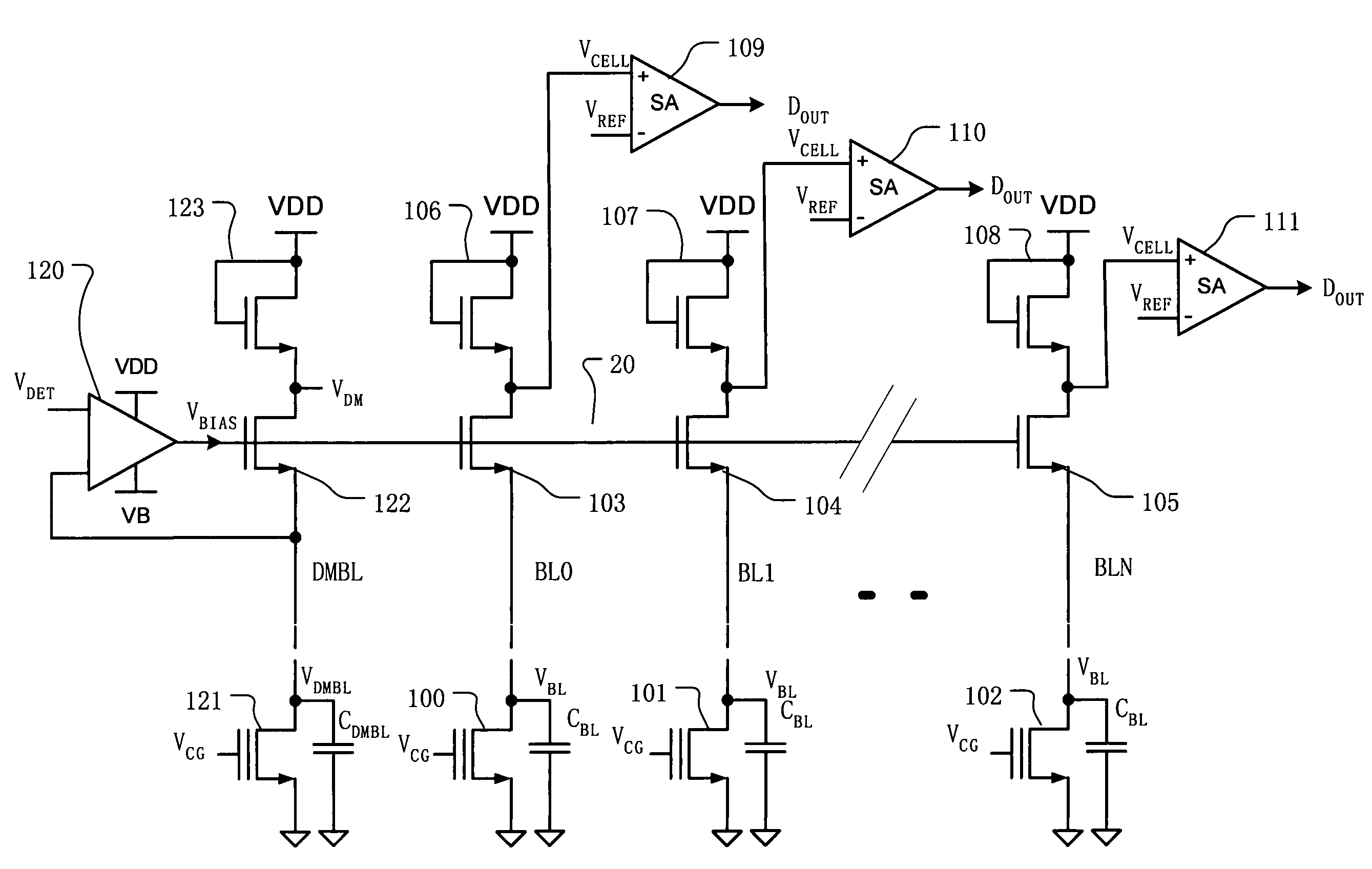
[0026]FIG. 4 illustrates sensing circuitry including a reference bit line DMBL (dummy bit line) and shared biasing circuitry for high speed and low power precharging. A memory array is represented by memory cells 100–102, found on respective columns in an array of memory cells, and selected for connection to bit lines by decoding circuitry not shown. Capacitor symbols CBL are illustrated, and associated with each of the bit lines. The capacitor symbols CBL represent the total bit line capacitance for access to a selected cell. In the illustrated embodiment, there are N bit lines, labeled BL0, BL1, . . . BLN in the array of memory cells. Clamp transistors 103–105 and load transistors 106–108 are included on respective bit lines BL0–BLN, and arranged identically in the illustrated embodiment. Clamp transistor 103 acts as a clamping circuit on bit line BL0. In this embodimen...


PUM


Abstract

An integrated circuit memory array with an extra column of memory cells and a reference bit line is provided, in which the reference bit line acts as a reference for a shared precharging and clamping control on the bit lines in the array. Clamp transistors are coupled to respective bit lines in the array, and adapted to prevent voltage on the respective bit lines from exceeding a target level. A comparator has an input coupled to the reference bit line and an output coupled to the clamp transistors on the plurality of bit lines. The comparator generates a bias voltage which turns on the clamp transistors at a first bias level when the reference bit line has a voltage below the target level, and a second bias level, which is lower than the first bias level, when the reference bit line has a voltage near the target level.

Description

BACKGROUND OF THE INVENTION[0001]1. Field of the Invention[0002]The present invention relates to integrated circuit memory devices, and to sense circuitry in such memory devices.[0003]2. Description of Related Art[0004]Integrated circuit memory devices are becoming smaller and faster. One limitation on the size and speed of memory devices arises from circuitry used for precharging and biasing bit lines in preparation for sensing data from the array. Typical structures used for these purposes are illustrated in U.S. Pat. No. 6,219,290, entitled MEMORY CELL SENSE AMPLIFIER, invented by Chang et al.; U.S. Pat. No. 6,498,751, entitled FAST SENSE AMPLIFIER FOR NONVOLATILE MEMORIES, invented by Ordonez, et al.; and U.S. Pat. No. 6,392,447, entitled SENSE AMPLIFIER WITH IMPROVED SENSITIVITY, invented by Rai et al.[0005]FIG. 1 illustrates a basic biasing structure used in prior art memory devices. The memory devices include a plurality of sense amplifiers, such as sense amplifiers 22, 23, 2...

Claims


Application Information

Patent Timeline
Patent Type & Authority Patents(United States)
IPC IPC(8): G11C7/00G11C16/06
CPCG11C16/24G11C7/12
Inventor CHOU, SHEREECHUEH, LUNG-YILIN, YU-SHEN
Owner MACRONIX INT CO LTD
Why Eureka
Try Eureka