Light emitting device using LED

a technology of light-emitting devices and led light-emitting elements, which is applied in the direction of semiconductor devices for light sources, discharge tubes luminescnet screens, lighting and heating apparatus, etc., can solve the problems of ineffective light-emitting, inability to efficiently apply light, and material or resin tend to quickly deteriorate, so as to prolong the service life of light-emitting devices and improve the heat-emitting property of light-emitting elements. , the effect o

Inactive Publication Date: 2006-08-01
MATSUSHITA ELECTRIC WORKS LTD
View PDF13 Cites 100 Cited by
  • Summary
  • Abstract
  • Description
  • Claims
  • Application Information

AI Technical Summary

Benefits of technology

[0007]With this arrangement, light emitted from the light-emitting element, is made incident on the fluorescent member to excite the fluorescent member, and to allow the fluorescent member to re-emit light having a wavelength that is different from that of the incident light (exciting light). This exciting light and light emitted from the fluorescent material are made incident on the optical member to be aligned in a predetermined direction based upon the optical shape of the optical member, and released outside the light-emitting device. Since the fluorescent member is not made in contact with the light-emitting element, the fluorescent member does not suffer from heat of the light-emitting element through heat conduction. Therefore, the heat that the fluorescent member receives from the light-emitting element is smaller than that in the case when the two members are made in contact with each other so that it is possible to suppress deterioration due to heat in the resin or the like that is a transparent substance in which the fluorescent material constituting the fluorescent member or the fluorescent material is dispersed and maintained, and consequently to lengthen the service life of the fluorescent member. Moreover, light from the light-emitting element is first made incident on the fluorescent member having a light-scattering property, and then made incident on the optical member; therefore, in comparison with the case in which, after having been made incident on the optical member, the resulting light is released outside through the fluorescent member, this arrangement allows the optical member to exert a light aligning function more effectively.
[0026]Preferably, in the improved invention, the fluorescent member is placed inside the concave section formed in the optical member. With this arrangement, the optical member can be placed closer to the substrate and the light-emitting element so that it is possible to easily design the optical shape of the optical member. Moreover, a concave section is formed in the optical member, and the entire surface with this concave section formed therein is coated with a fluorescent member, and an excessive amount of the fluorescent member is wiped with, for example, squeegee or the like; thus, with these manufacturing processes, the fluorescent member is uniformly formed in the concave section. Consequently, it is possible to get light-emitting devices among which color irregularities are alleviated, and it is also possible to simplify the manufacturing processes as compared with the conventional method; thus, it becomes possible to improve the manufacturing cost reduction effects. In particular, this arrangement is effective when applied to a light-emitting device having a plurality of light-emitting elements integrally formed therein.

Problems solved by technology

In the above-mentioned light-emitting device using LED, however, since the fluorescent material or the fluorescent-material-mixed resin is made in contact with the LED chip, that is, the light-emitting element, the material or resin tends to quickly deteriorate due to heat from the light-emitting element, and a problem results that the service life of the light-emitting device using LED depends on the service life of the fluorescent material or the fluorescent-material-mixed resin and dose not depend on the service life of the LED chip itself.
However, in these cases, the fluorescent member 30, which has a light scattering property, is placed outside the optical member 40; consequently, even when an attempt is made to converge light rays from the light-emitting element 20 by using the optical member 40, and to align light rays in a predetermined direction, the light rays are scattered by the fluorescent member 30, and problems are caused that desired light-ray alignment is not achieved and it is not possible to efficiently apply light.

Method used


Image

  • Light emitting device using LED
  • Light emitting device using LED
  • Light emitting device using LED

Examples


embodiment 1

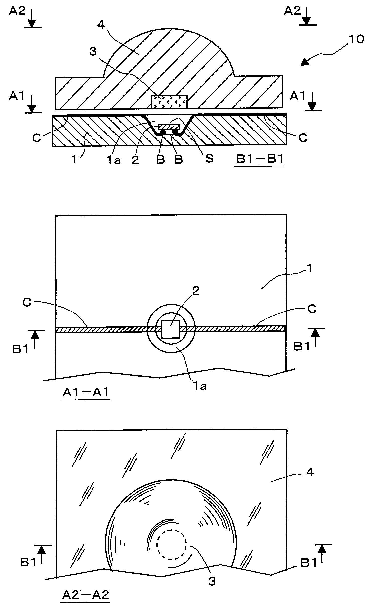
[0061]Referring to FIGS. 1 through 3, the following description discusses embodiment 1 of the present invention. The light-emitting device 10 of the present embodiment is provided with a light-emitting element 2 which is placed on a bottom surface of a concave section 1a that has a reversed cone shape with a trapezoidal shape in its cross-section and is formed on one surface of a flat-plate-shaped packaging substrate 1, an optical member 4 having a flat surface that is aligned face to face with the surface of the packaging substrate 1 on which this light-emitting element 2 is placed, and a disc-shaped fluorescent member 3 that is embedded in a concave section formed in the center portion of the surface belonging with the optical member 4 and facing the packaging substrate 1 so as to be flush with the above-mentioned surface of the optical member 4. The light-emitting element 2 is a blue-light-emitting LED, and is mounted with its face down, and the electrode patterns of the light-em...

embodiment 2

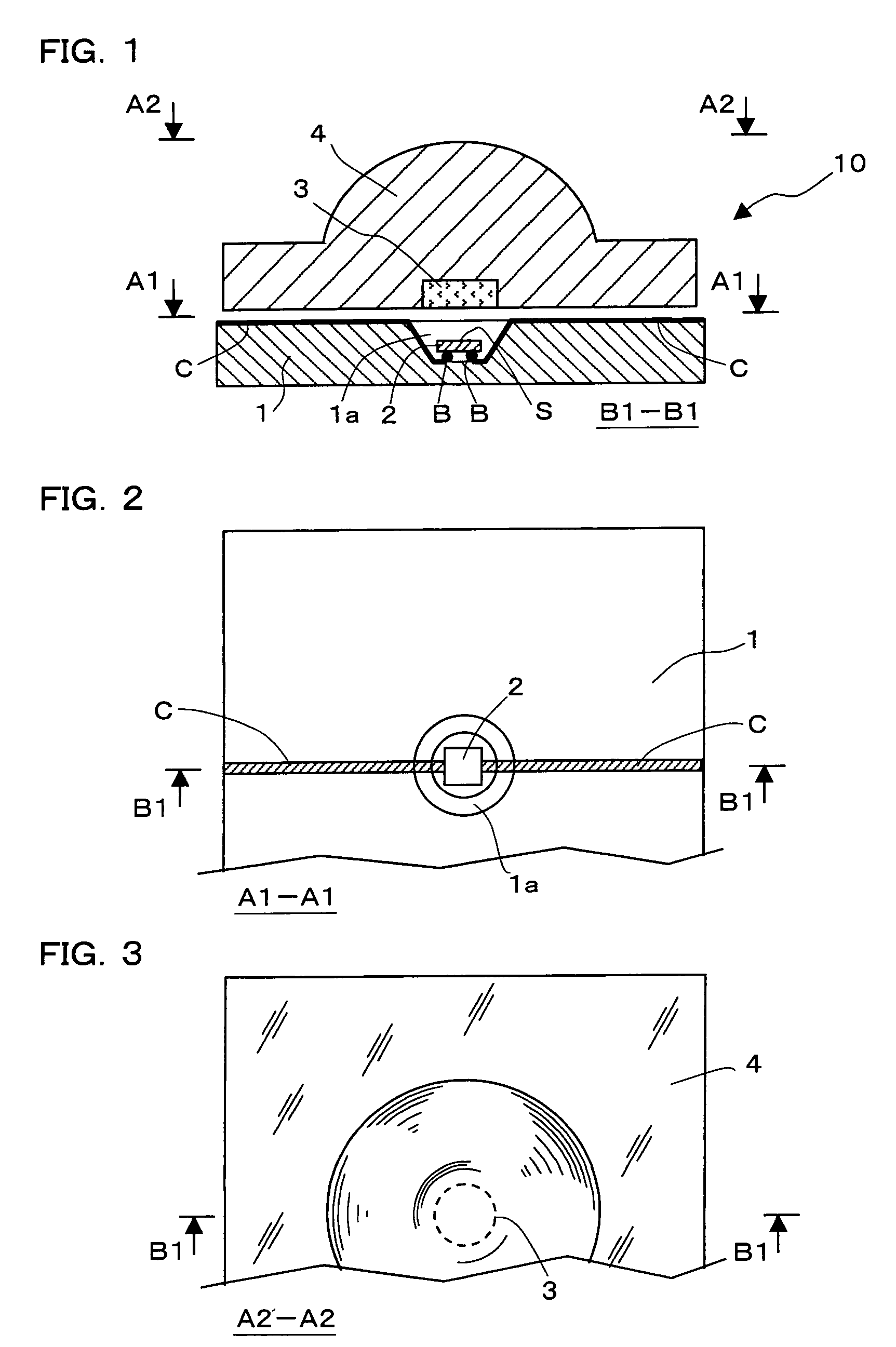
[0068]Referring to FIG. 4 and FIG. 5, the following description discusses embodiment 2 of the present invention. A step portion is formed on the upper portion of the opening of the concave section 1a in the packaging substrate, which is formed as a section in which the light-emitting element 2 is placed, and the fluorescent member 3 is fitted and detachably attached to this step portion. With this arrangement, only the fluorescent member that tends to deteriorate faster in comparison with other parts can be exchanged so that it becomes possible to further lengthen the service life of the light-emitting device.

embodiment 3

[0069]Referring to FIG. 6 and FIG. 7, the following description discusses embodiment 3 of the present invention. In the light-emitting device of the present embodiment, as shown in FIG. 6, the optical member 4 has a convex lens shape formed into a shell shape. With this optical shape, light a1, emitted from the fluorescent member 3, is formed into light a2 that is refracted so as to be converged in the center direction of the light-emitting device 10, and aligned on the surface of the optical part 4.

[0070]Moreover, as shown in FIG. 7, in a light-emitting device 10 in which a plurality of light-emitting elements 2 are assembled on the packaging substrate with multi-lenses 4m that form respective convex lenses being placed as the optical members 4 with respect to the light-emitting elements 2, by using a plurality of the light-emitting elements 2, the device is capable of applying a more quantity of light outside the device. The optical member 4 having such a structure with multiple l...


PUM


Abstract

A light-emitting device which uses and LED having a light-emitting element being placed on a package substrate. The light-emitting element has a light-extracting surface. A fluorescent element which is formed by dispersing a fluorescent material in a transparent substance and is placed face to face with the light-extracting surface of the light emitting element and comprises a clearance gap in between. The light-emitting element generates light of a certain wavelength that emanates through the light-extracting surface into the fluorescent element where the wavelength is changed. The device further comprises an optical element which receives light from the light-emitting element through the fluorescent element and directs the light to the outside of the device.

Description

TECHNICAL FIELD[0001]The present invention relates to a light-emitting device that generates mixed color light by using a light-emitting element and a fluorescent material.BACKGROUND ART[0002]In recent years, a light-emitting diode (LED) chip that emits blue or ultraviolet light by using a gallium nitride-based compound semiconductor has been developed. Further, by combining the LED chip with various fluorescent materials, light-emitting devices using LED have been developed which can emit light having color hues different from light emitted by the LED chip, such as white light. The light-emitting devices using LED have advantages of small size, little weight and power saving in comparison with light-emitting devices using hot filaments or gas discharges, and have been currently used widely as devices such as light-sources for indication, substitution for small-size light bulbs, and light-sources for liquid crystal display panels. The prior art devices of this type are disclosed in ...

Claims


Application Information

Patent Timeline
Patent Type & Authority Patents(United States)
IPC IPC(8): H01L29/22H01L29/24F21V29/02H01L33/50H01L33/54H01L33/58H01L33/60
CPCF21K9/00H01L33/507H01L33/54F21V29/83F21V29/677H01L33/60F21K9/56H01L33/58F21K9/64H01L2224/16225
Inventor SUGIMOTO, MASARUYAMAGUCHI, MASAOHASHIMOTO, TAKUMANISHIOKA, KOJIYOKOTANI, RYOJIKIMURA, HIDEYOSHIMURAKAMI, TADASHISHIOHAMA, EIJI
Owner MATSUSHITA ELECTRIC WORKS LTD
Why Eureka
Try Eureka