Parallel field effect transistor structure having a body contact
- Summary
- Abstract
- Description
- Claims
- Application Information
AI Technical Summary
Benefits of technology
Problems solved by technology
Method used
Image

Examples
Embodiment Construction
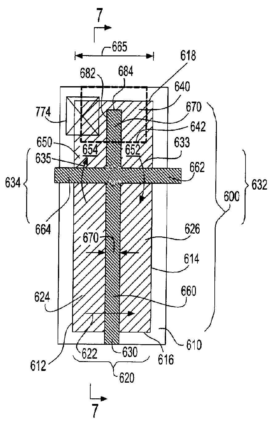
[0030]In accordance with the embodiments of the invention, a semiconductor device structure and fabrication method are provided which address the foregoing problems of body-contacted FETs. With reference to FIG. 6, in the semiconductor device structures described herein, a first field effect transistor (FET) 620 is disposed in a unitary single-crystal semiconductor region 600 of a substrate. A body contact 640 has a junction 642 to a diffusion region 650 of the unitary single-crystal region 600 that is not electrically tied to the source region 624 of the first FET or indeed to the drain region 626 of the first FET. Instead, the diffusion region 650 functions as at least one of a source region and a drain region of a second FET 632 and that of another second FET 634 having a source-drain conduction path to at least one of the first source region and first drain region of the first FET. In such way, the source-drain conduction path of the second FET is electrically connected in paral...
PUM
 Abstract
Description
Claims
Application Information
 - R&D
- Intellectual Property
- Life Sciences
- Materials
- Tech Scout
- Unparalleled Data Quality
- Higher Quality Content
- 60% Fewer Hallucinations
Browse by: Latest US Patents, China's latest patents, Technical Efficacy Thesaurus, Application Domain, Technology Topic, Popular Technical Reports.
© 2025 PatSnap. All rights reserved.Legal|Privacy policy|Modern Slavery Act Transparency Statement|Sitemap|About US| Contact US: help@patsnap.com