

Electrostatic discharge protection component
a protection component and electrostatic discharge technology, applied in the direction of overvoltage protection resistors, emergency protective arrangements for limiting excess voltage/current, mechanical equipment, etc., can solve the problem of insufficient bypassing effect, inability to bypass electrostatic discharge occurring in about 0.5 to 2 nanoseconds, and increase the number of breakdown accidents of electric circuits inside the appliance, etc. problems, to achieve the effect of preventing electrostatic discharge pulses, reducing the voltage applied to the protected circuit, and high impedan
- Summary
- Abstract
- Description
- Claims
- Application Information
AI Technical Summary
Benefits of technology
Problems solved by technology
Method used
Image

Examples
first exemplary embodiment
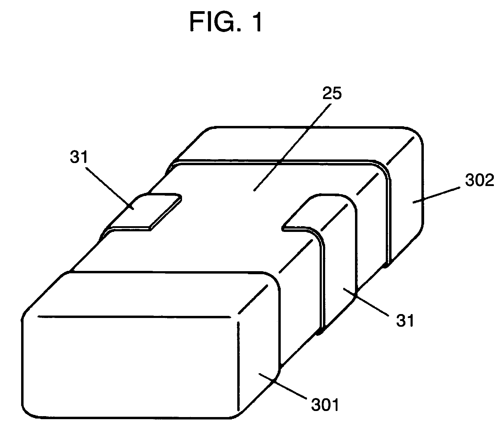
[0034]FIG. 1 is an outline perspective view of a protection component in exemplary embodiment 1 of the invention, and FIG. 2 is a schematic perspective exploded view of ceramic sinter for composing this protection component. FIG. 3 is an equivalent circuit diagram of the protection component.
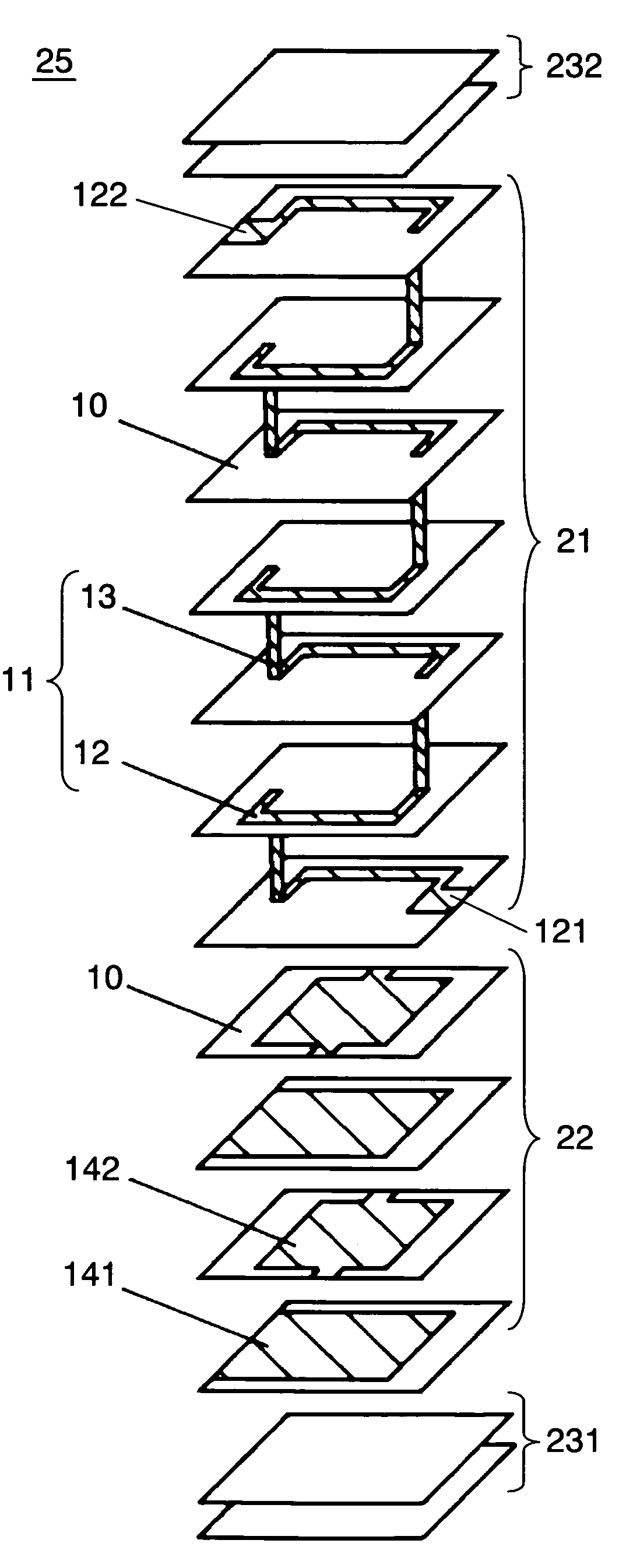
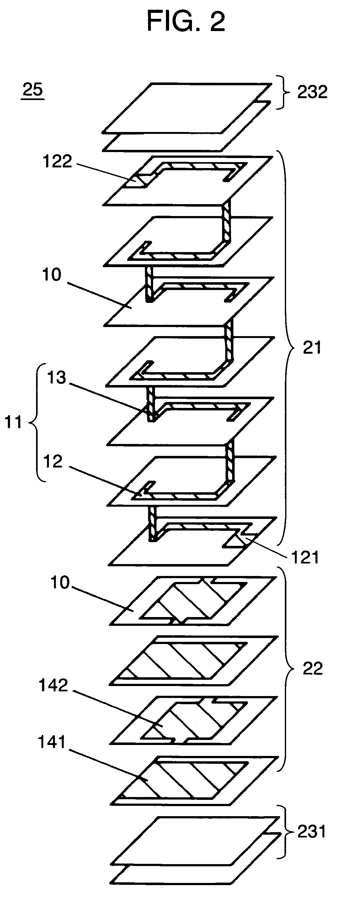
[0035]The protection component of the invention comprises an external electrode for input 301 and an external electrode for output 302 disposed at both shorter sides of a ceramic sinter 25, and external electrodes for grounding 31 disposed at both longer sides. The internal structure of the ceramic sinter 25 is shown in FIG. 2. The ceramic sinter 25 is an integrated laminated body of varistor 22, inductor 21, and cover layers 231, 232 as surface protective layers.
[0036]The inductor 21 includes a wiring conductor 12 formed in a ceramic layer 10, and a via conductor 13 filling up a via (not shown) opened in the ceramic layer 10, which are connected together to form a spiral coil conductor 11, and ...
second exemplary embodiment
[0059]FIG. 10 is a schematic perspective exploded view of ceramic sinter 40 for composing a protection component in exemplary embodiment 2 of the invention. FIG. 11 is an equivalent circuit diagram of this protection component. What the protection component of this exemplary embodiment differs from the protection component in exemplary embodiment 1 lies in the structure of the ceramic sinter. That is, in this exemplary embodiment, it is characteristic that the ceramic sinter has one inductor and two varistors. The outline shape of the protection component of the exemplary embodiment is same as exemplary embodiment 1 shown in FIG. 1, and FIG. 1 is cited as required. Same constituent components are identified with same reference numerals.
[0060]A ceramic sinter 40 composing the protection component of the exemplary embodiment is an integrated laminated body of first varistor 221, second varistor 222, inductor 21, and cover layers 231, 232 as surface protective layers.
[0061]The inductor...
third exemplary embodiment
[0078]A protection component in exemplary embodiment 3 of the invention is described specifically below while referring to the drawings. FIG. 14 is a schematic perspective exploded view of ceramic sinter 50 for composing a protection component in this exemplary embodiment. FIG. 15 is an equivalent circuit diagram of this protection component.
[0079]What the protection component of this exemplary embodiment differs from the protection component in exemplary embodiment 1 and exemplary embodiment 2 lies in the structure of the ceramic sinter. That is, in this exemplary embodiment, it is characteristic that the ceramic sinter has two inductors and three varistors. The outline shape of the protection component of the exemplary embodiment is same as exemplary embodiment 1 and exemplary embodiment 2, and FIG. 1 is cited when describing the outline structure. Same constituent components as in exemplary embodiment 1 and exemplary embodiment 2 are identified with same reference numerals.
[0080]...
PUM
| Property | Measurement | Unit |
|---|---|---|
| Time | aaaaa | aaaaa |
| Frequency | aaaaa | aaaaa |
| Frequency | aaaaa | aaaaa |
Abstract
Description
Claims
Application Information