Method for preparing low dielectric films

a dielectric film and low-dielectric technology, applied in the field of low-dielectric film preparation, can solve problems such as signal delay

Inactive Publication Date: 2006-08-08
POSTECH ACAD IND FOUND
View PDF10 Cites 33 Cited by
  • Summary
  • Abstract
  • Description
  • Claims
  • Application Information

AI Technical Summary

Benefits of technology

[0005]It is, therefore, an object of the present invention to provide a method for preparing an improved low dielectric constant hydrogenated silicon-oxycarbide (SiCO:H) film using a chemical vapor deposition (CVD) technique.
[0006]It is another object of the present invention to provide a SiCOH film having a dielectric constant (k) lower than those of conventional low dielectric materials.
[0007]In accordance with one aspect of the present invention, there is provided a method for preparing a low dielectric constant hydrogenated silicon-oxycarbide (SiCO:H) film which comprises conducting chemical vapor deposition using, together with an O2-containing gas plasma, an organosilicon or organosilicate compound having at least one vinyl or ethinyl group, or a mixture of a saturated organosilicon or organosilicate compound and an unsaturated hydrocarbon.
[0008]In accordance with another aspect of the present invention, there is provided a low dielectric constant SiCOH thin film having a dielectric constant (k) of 2.6 or below, prepared by said method.

Problems solved by technology

With ever decreasing size of electronic devices utilized in ULSI (ultra-large-scale integrated) circuits, there has emerged the problem of increased capacitance of intralayers and / or interlayers, causing signal delays.

Method used


Image

  • Method for preparing low dielectric films
  • Method for preparing low dielectric films
  • Method for preparing low dielectric films

Examples


example 1

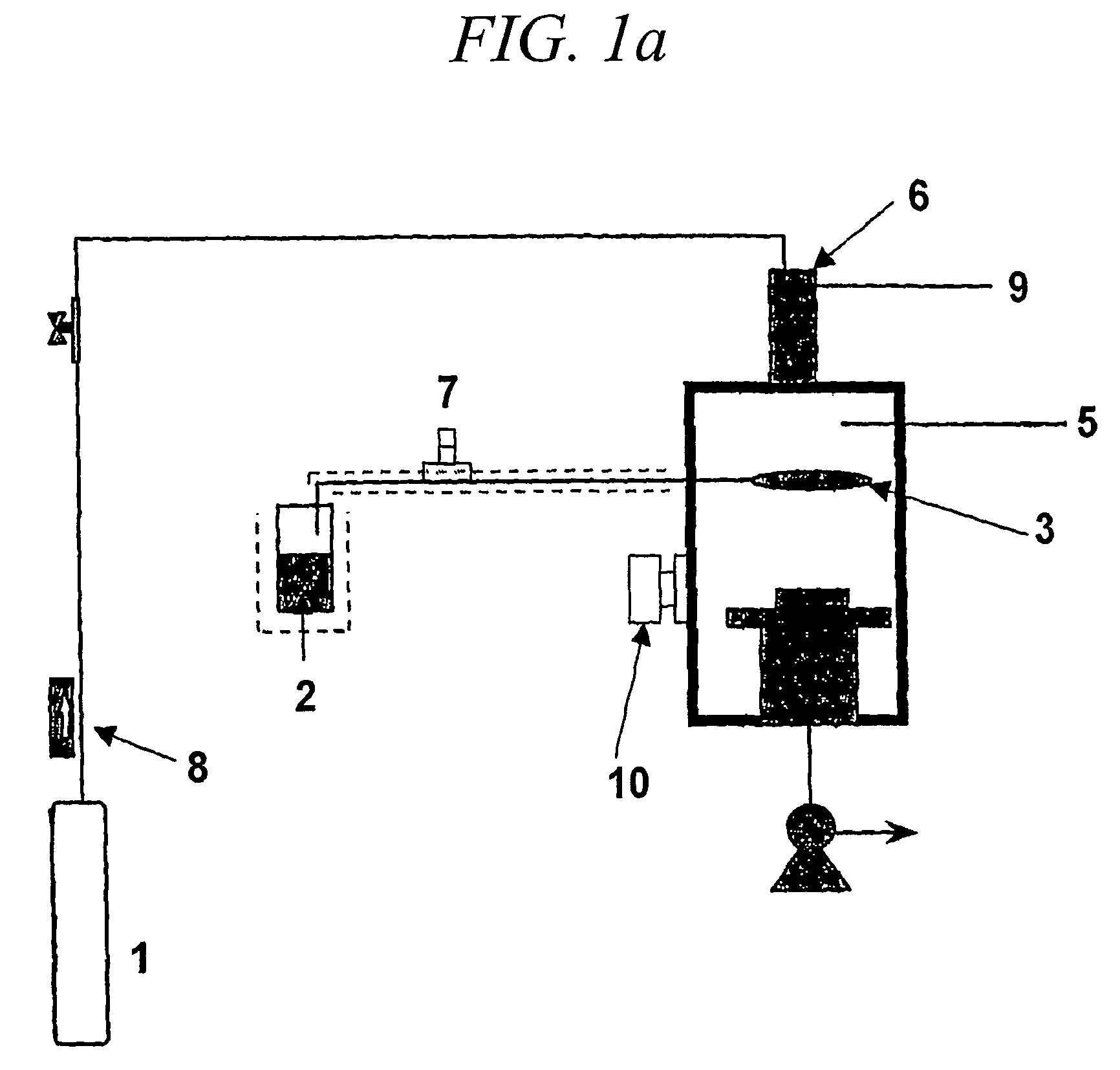
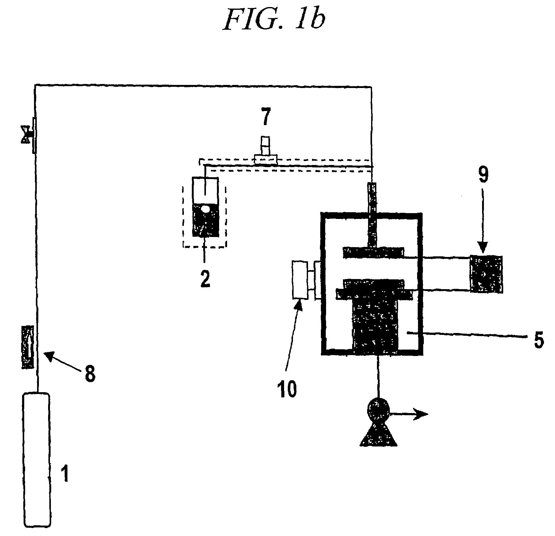
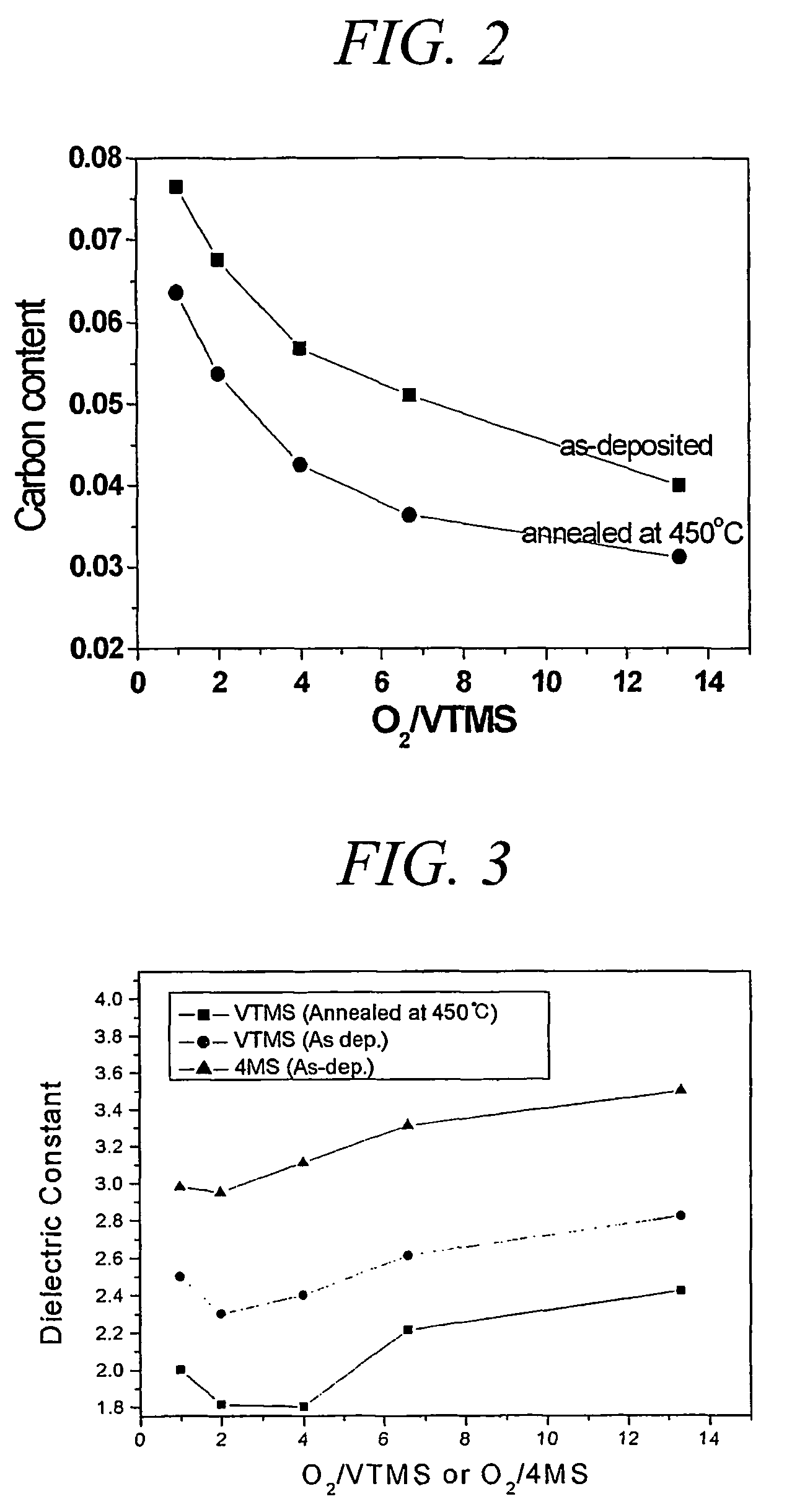
[0045]A SiCOH film was deposited on a Pt substrate using vinyltrimethylsilane (VTMS, SiC5H12) and O2 in the direct plasma apparatus shown in FIG. 1b. The flow ratio of O2 / VTMS was varied in the range of 1 to 13.3 during the film deposition. The pressure and temperature in the reactor were 1 mmHg and 30° C., respectively, and the applied plasma power, 60W. The film so deposited was annealed under an Ar atmosphere at a temperature in the range of 300 to 500° C., to obtain a low dielectric constant film.

[0046]As shown in FIG. 2, the respective carbon contents of the deposited film and the film annealed at 450° C. become lower with the increasing flow ratio of O2 / VTMS. FIG. 3 exhibits that the annealed film at 450° C. has a dielectric constant ranging from 1.8 to 2.4, while the deposited film without the annealing has a dielectric constant ranging from 2.3 to 2.8. FIGS. 4 and 5 show the changes in the dielectric constant of the film obtained in Example 1 with the changes in the annealin...

example 2

[0048]Except that a mixture of tetramethylsilane(4MS, SiC4H12) and C2F4 (1:1) was used instead of VTMS, the procedure of Example 1 was repeated to obtain a deposited film, which was subsequently annealed.

[0049]FIG. 6 and FIG. 7 show the carbon contents and dielectric constants of the deposited film and the annealed film, respectively. The deposited film has a dielectric constant of 3.0 or below, and the film annealed at 450° C. has a dielectric constant of 2.5 or below. FIG. 8 and FIG. 9 show the effects of the annealing temperature (annealing time=0.5 hr) and annealing time (annealing temperature=400° C.) at the O2 / (4MS+C2F4) flow ratio of 4 on the dielectric constant of the film, respectively. The film annealed at 300 to 500° C. for 0.5 hr has a dielectric constant of 2.75 or below.

example 3

[0050]The procedure of Example 1 was repeated using tetravinyltetramethylcyclotetrasiloxaneC (TVMCTSO, Si4O4C12H24) in place of VTMS, to obtain a deposited film which was subsequently annealed.

[0051]FIG. 10 and FIG. 11 show the carbon contents and dielectric constants of the deposited film and the annealed film, respectively. The deposited film has a dielectric constant of 2.4 or below, and the film annealed at 450° C., a dielectric constant of 2.2 or below. FIG. 12 and FIG. 13 show the effects of the annealing temperature (annealing time=0.5 hr) and annealing time (annealing temperature=450° C.) at the O2 / TVTMCTSO flow ratio of 4 on the dielectric constant of the film, respectively. The film annealed at 300 to 500° C. for 0.5 hr has a dielectric constant of 2.1 or below.


PUM

PropertyMeasurementUnit
dielectric constantaaaaaaaaaa
temperatureaaaaaaaaaa
dielectric constantaaaaaaaaaa

Abstract

A low dielectric constant hydrogenated silicon-oxycarbide (SiCO:H) film is prepared by bringing an organosilicon or organosilicate compound having at least one vinyl or ethynyl group, or a mixture of a saturated organosilicon or organosilicate compound and an unsaturated hydrocarbon into contact with a substrate in the presence of an O2-containing gas plasma.

Description

FIELD OF THE INVENTION[0001]The present invention relates to an improved plasma chemical vapor deposition (CVD) method for preparing a low dielectric constant hydrogenated silicon-oxycarbide (SiCO:H) film.BACKGROUND OF THE INVENTION[0002]With ever decreasing size of electronic devices utilized in ULSI (ultra-large-scale integrated) circuits, there has emerged the problem of increased capacitance of intralayers and / or interlayers, causing signal delays. Therefore, there has been a need to develop a low dielectric constant (k) material having a k-value lower than that of the conventional silicon dioxide (SiO2) or fluorinated silicon oxide (SiOF).[0003]U.S. Pat. No. 6,147,009 discloses a low dielectric constant material produced by reacting the vapor of a precursor containing atoms of Si, C, O and H in a parallel plate plasma enhanced chemical vapor deposition chamber, the precursor being a molecule with a ring structure such as 1,3,5,7-tetramethylcyclotetrasiloxane(TMCTS, C4H16O4Si4),...

Claims


Application Information

Patent Timeline
Patent Type & Authority Patents(United States)
IPC IPC(8): H05H1/24C23C16/42C23C16/30C23C16/40H01L21/31H01L21/312H01L21/316H01L25/00
CPCC23C16/30C23C16/401H01L21/02126H01L21/31633H01L21/02216H01L21/02274H01L21/3122H01L21/02211H01L21/31
Inventor RHEE, SHI-WOOKWAK, SANG-KI
Owner POSTECH ACAD IND FOUND
Why Eureka
Try Eureka