Method for packaging small size memory cards

a memory card and small-size technology, applied in the direction of printed circuit aspects, electrically conductive connections, electrical apparatus, etc., can solve the problems of pcb flexing, pcb flexing, and the space behind the contact pads, which is also frequently subject to stress, and achieves the effect of preventing flexing

Inactive Publication Date: 2006-08-15
ELEX P IND
View PDF5 Cites 29 Cited by
  • Summary
  • Abstract
  • Description
  • Claims
  • Application Information

AI Technical Summary

Benefits of technology

[0007]The invention further allows the memory card to be packaged in a housing without the need for tolerances to fit the corresponding component profile of the populated PCB therewithin. The resultant moulded card according to the invention further provides for a sturdy, integral packaging, which prevents the assembled card from flexing under stress.
[0009]The moulding method of the invention is not limited by minimum thickness of individual housing pieces, thus maximises the internal space, particularly thickness, of the memory card available for populating chips on the PCB.STATEMENT OF INVENTION
[0013]Preferably still, the tie bar extends to a peripheral frame which integrally and substantially surrounds the populated PCB, thereby holding the populated PCB in place in the cavity of the one mould piece by securing a portion of the peripheral frame. The peripheral frame may preferably be provided with a plurality of tie bars, which are optimally distributed around said peripheral frame to prevent flexure of said populated PCB as it is held within the mould piece.

Problems solved by technology

Such spaces, in turn, enable the assembled card to flex under stress, which may eventually lead to the 2-piece housing to delaminate, crack, separate, and / or solder joints of the components on the PCB to deteriorate or weaken due to the flexing of the PCB.
Another weakness of this conventional construction is the space behind the contact pads, which is also frequently subjected to stress as the card is inserted into a device to be read and removed.
Some form of padding or reinforcement is required behind this area to counter the stress, which otherwise may cause the PCB to flex within the housing.
Minimum wall thickness is limited by the high pressure required to fill at a large width-to-thickness ratio, as well as difficulty in removing thin parts from the mould.

Method used


Image

  • Method for packaging small size memory cards
  • Method for packaging small size memory cards
  • Method for packaging small size memory cards

Examples


Embodiment Construction

[0027]The following description discloses the specific embodiment of a Secure Digital (SD) card as an example application of the method of the invention. It is to be understood that the method is applicable to other types of small size memory cards including SmartMedia™ (SM) card, Multimedia card (MMC), CompactFlash™ (CF) card, PC card, Memory Stick™, xD Picture card and like small size memory cards which formats and specifications may be introduced in the future.

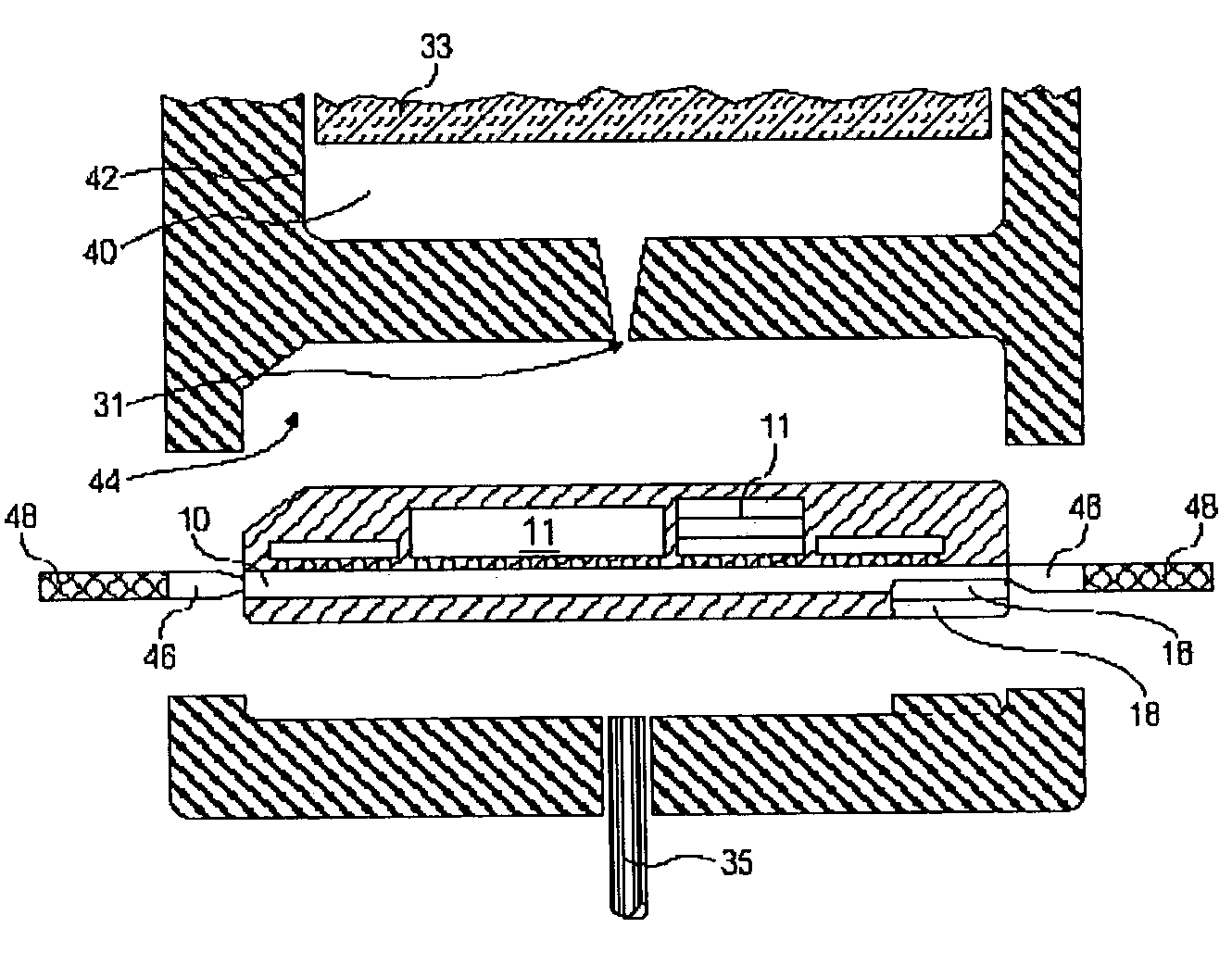
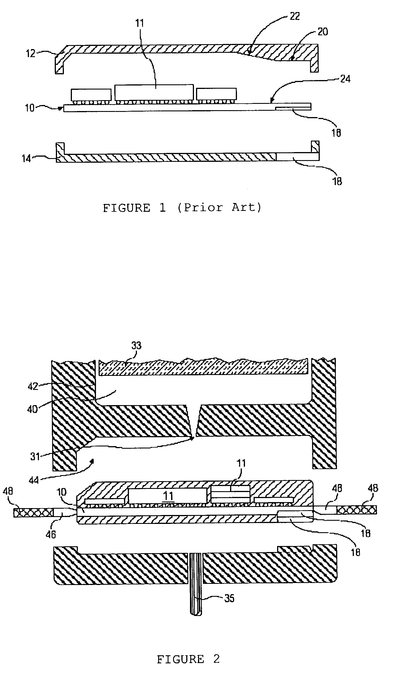
[0028]FIG. 2 shows in cross-sectional view a suggested arrangement of the moulding process enabling the encapsulation of the populated PCB (10). The general embodiment comprises providing the populated PCB in a mould, which has been tooled to form the standard external dimensions and features of the designated memory card, and then push an amount of moulding polymer (40) at high pressure into the mould cavity to flow over both sides of the populated PCB (10) and encapsulate it.

[0029]Although various moulding techniques such...


PUM

PropertyMeasurementUnit
sizeaaaaaaaaaa
dimensionsaaaaaaaaaa
stressaaaaaaaaaa

Abstract

A method is disclosed for packaging a small size memory card, including xD Picture card, Memory Stick™, Secure Digital™ (SD) card, SmartMedia™ (SM) card, Multimedia card (MMC), CompactFlash™ (CF) card and PC card, by moulding over to encapsulate a populated printed circuit board (PCB) (10) to form the standard external dimensions and features of the memory card.The method comprises holding the populated PCB (10) in place in a cavity (44) of at least one mould piece; and moulding over both sides of the populated printed circuit board (10) to encapsulate said board. Various embodiments are disclosed, including means for holding the populated PCB (10) in the moulding cavity (44) for the encapsulation process, which includes transfer moulding and injection moulding processes, one or more moulding steps, and moulding over one part of one side of said board before the other side, and / or simultaneously moulding over both sides of said board.

Description

TECHNICAL FIELD[0001]This invention relates to a method for forming a small size memory card, including Secure Digital™ (SD) card, SmartMedia™ (SM) card, Multimedia card (MMC), CompactFlash™ (CF) card, PC card, Memory Stick™ and xD Picture card by moulding or encapsulation.BACKGROUND ART[0002]Small size memory card, including xD Picture card, Secure Digital™ (SD) card, SmartMedia™ (SM) card, Multimedia card (MMC), CompactFlash™ (CF) card and PC card are assembled by first making the printed circuit board (PCB) with the contact pads and mounting points for components including microchips (11) such as flash memory, micro-controller, etc. to be mounted thereunto as shown schematically in FIG. 1 (Prior Art). Once the components are mounted, the populated PCB (10) is then fitted into a 2-piece plastic or metal housing (12, 14) which may be snapped fit to close and sealed by microwave or ultrasound leaving certain parts such as the contact pads (16) exposed via openings (18).[0003]In addi...

Claims


Application Information

Patent Timeline
Patent Type & Authority Patents(United States)
IPC IPC(8): H05K3/30H05K1/14H05K1/11H05K3/00H05K3/28
CPCH05K3/284H05K1/117H05K3/0052H05K2201/10204H05K2203/1316Y10T29/49147Y10T29/49146Y10T29/49789Y10T29/4913Y10T29/49126Y10T29/49798Y10T29/49171
Inventor FONG, PIAUYEW, CHEE KIANGLUM, COLIN CHUN SINGCHUA, MATTHEW KENG SIEW
Owner ELEX P IND
Why Eureka
Try Eureka