
Process flow for a performance enhanced MOSFET with self-aligned, recessed channel

a technology of mosfet and process flow, which is applied in the direction of semiconductor devices, electrical devices, transistors, etc., can solve the problems of reducing the performance of the transistor, so as to improve the inter-electrode capacitance, the effect of reducing the cost of the transistor

Active Publication Date: 2006-08-15
CHARTERED SEMICONDUCTOR MANUFACTURING +1
View PDF5 Cites 26 Cited by
  • Summary
  • Abstract
  • Description
  • Claims
  • Application Information

AI Technical Summary

Benefits of technology

[0013]Another object of the present invention is to provide a method for forming a self-aligned, recessed channel, MOSFET device that alleviates the problems due to short channel effects, including punch through, hot carrier effect and increased inter-electrode capacitance.
[0014]Another object of the present invention is to provide a method for forming a self-aligned, recessed channel, MOSFET gate electrode that alleviates the problems due to short channel effects, including punch through, hot carrier effect and increased inter-electrode capacitance.
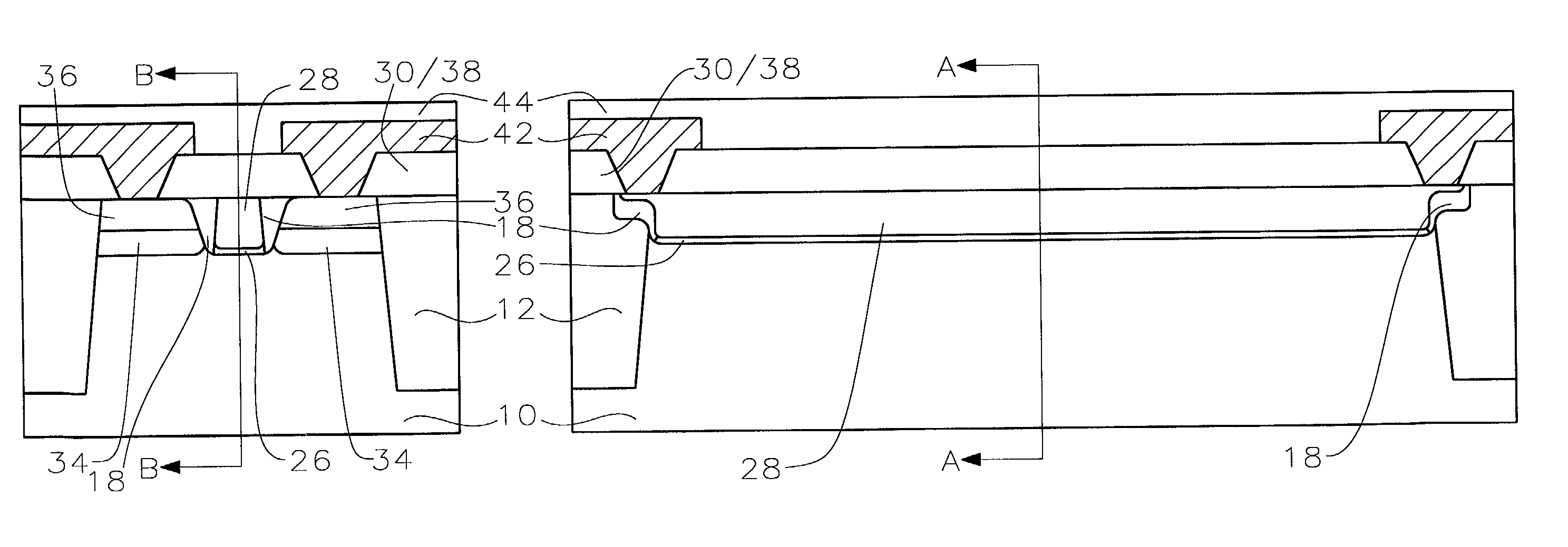
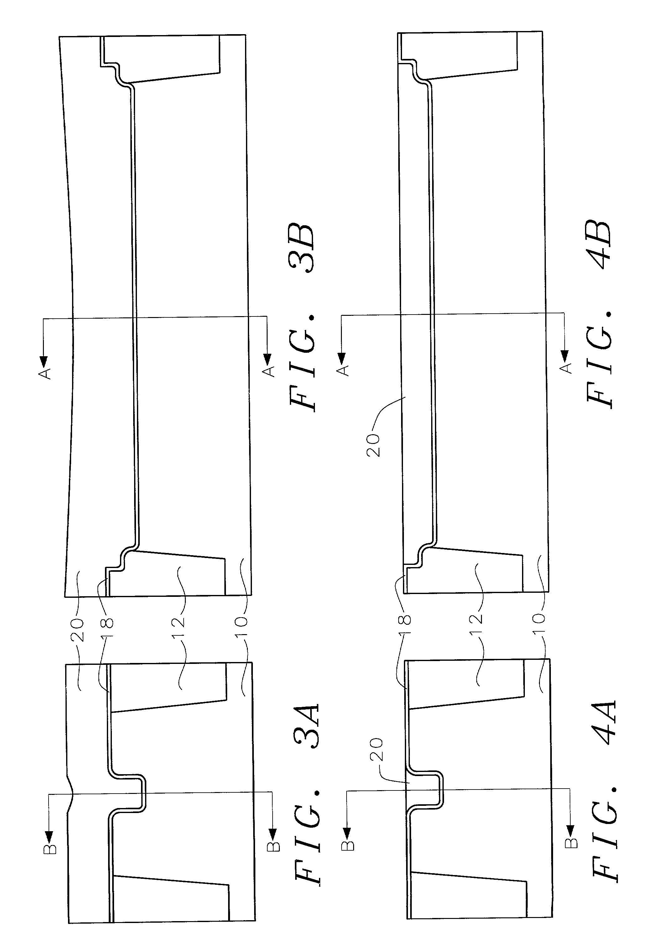
[0016]A thin pad oxide layer is grown overlying the surface followed by deposition of a thick silicon nitride layer covering the surface and filling the gate recess. The top surface is then planarized exposing the pad oxide layer. Additional oxide is grown causing the pad oxide layer to thicken. A portion of the silicon nitride layer is etched away and additional oxide is grown causing the pad oxide layer to further thicken. This forms a tapered oxide layer along the sidewalls of the gate recess. The remaining silicon nitride layer is then removed, re-opening the gate recess. A threshold adjust and punch-through implantation is performed into the substrate below the gate recess. The tapered oxide layer on the gate recess sidewalls protects the implantation from reaching areas laterally outside the forthcoming gate structure. Next, the pad oxide layer is isotropically etched to remove the oxide at the bottom of the gate recess. A gate dielectric is then grown in the bottom of the gate recess. This is followed by a deposition of gate polysilicon covering the top surface and filling the gate recess. The top surface is again planarized to expose the top of the substrate. This completes the formation of the recessed gate structure.

Problems solved by technology

As integrated circuit device dimensions are reduced, parasitic effects become a challenge.
In MOSFET devices, as the distance between the source and drain (channel length) is reduced, punch-through, hot-carrier effect, and interelectrode capacitance become factors that degrade performance.
This punch-through effect reduces the control the gate electrode has over the drain current.
This increase in drain capacitance limits the speed at which the device and the integrated circuit will switch.

Method used


Image

  • Process flow for a performance enhanced MOSFET with self-aligned, recessed channel
  • Process flow for a performance enhanced MOSFET with self-aligned, recessed channel
  • Process flow for a performance enhanced MOSFET with self-aligned, recessed channel

Examples


Embodiment Construction

[0020]This embodiment describes formation of a 100 nm recessed gate electrode in an n-channel (NMOS) or p-channel (PMOS) transistor. It will be understood by those skilled in the art that the invention can be extended to the formation of gate electrode structures of different sizes on a semiconductor wafer.

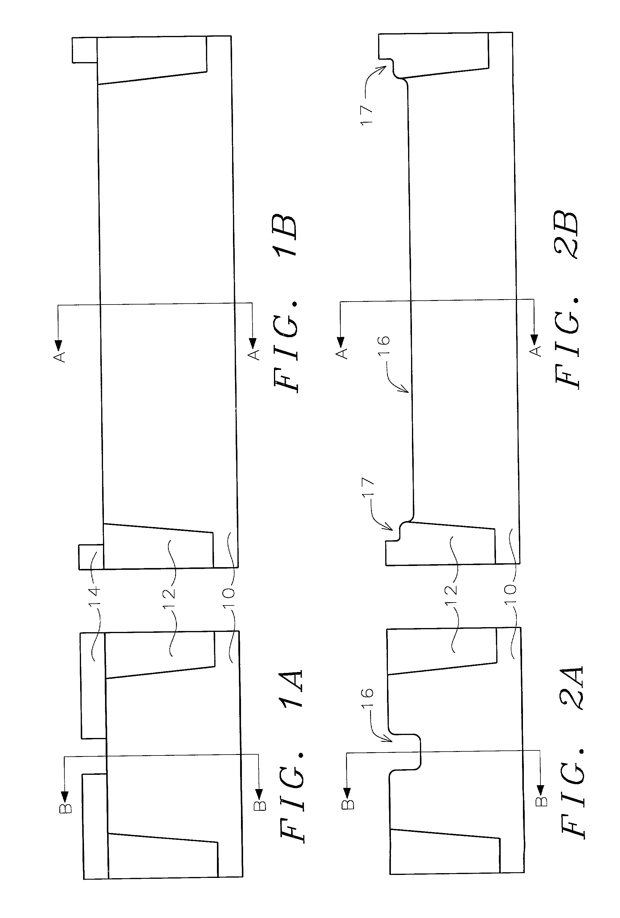
[0021]Referring now to FIG. 1 through FIG. 12, depicting schematically one embodiment of the present invention. Cut line “a” corresponds to each respective side view in FIG. 1a through FIG. 12a. Cut line “b” on each of the figures corresponds to each respective lateral side view shown in FIG. 1b through FIG. 12b.

[0022]Refer now more particularly to FIG. 1 where a partially formed MOS transistor is represented. A substrate 10 with a crystal orientation, for example, is provided. For an NMOS device, the substrate 10 is composed of p-type silicon; for a PMOS device, the substrate 10 is composed of n-type silicon. Shallow trench isolation (STI) regions 12 comprised of silicon oxide ...


PUM


Abstract

A method for forming a self-aligned, recessed channel, MOSFET device that alleviates problems due to short channel and hot carrier effects while reducing inter-electrode capacitance is described. A thin pad oxide layer is grown overlying the substrate and a gate recess, followed by deposition of a thick silicon nitride layer filling the gate recess. The top surface is planarized exposing the pad oxide layer. An additional oxide layer is grown, thickening the pad oxide layer. A portion of the silicon nitride layer is etched away and additional oxide layer is again grown. This forms a tapered oxide layer along the sidewalls of the gate recess. The remaining silicon nitride layer is removed. The oxide layer at the bottom of the gate recess is removed and a gate dielectric layer is grown. Gate polysilicon is deposited filling the gate recess. S / D implantations, metallization, and passivation complete fabrication of the device.

Description

[0001]This application is a DIV of Ser. No. 09 / 671,509 Sep. 27, 2002, U.S. Pat. No. 6,391,720.BACKGROUND OF THE INVENTION[0002](1) Field of the Invention[0003]The invention generally relates to a method of fabricating a semiconductor device and, more particularly, to a method of fabricating a field-effect transistor (FET) having a recessed gate structure in the manufacture of integrated circuits.[0004](2) Description of Prior Art[0005]A device prevalent in high-speed integrated circuits is the so-called metal-oxide-semiconductor field effect transistor (MOSFET). A MOSFET comprises three electrodes: a source, a drain and a gate. The heavily doped source and drain (S / D) regions are separated by a lightly doped channel. If the S / D are n-type material, then the channel is p-type and the device is an NMOS transistor. Conversely, if the S / D are p-type material, then the channel is n-type and a PMOS transistor results. The gate electrode is positioned over, but electrically insulated from ...

Claims


Application Information

Patent Timeline
Patent Type & Authority Patents(United States)
IPC IPC(8): H01L21/336H01L29/78
CPCH01L29/66545H01L29/7834H01L29/66621
Inventor SNEELAL, SNEEDHARAN PILLAIPOH, FRANCISLEE, JAMESSEE, ALEXLAU, C. K.SAMUDRA, GANESH SHANKAR
Owner CHARTERED SEMICONDUCTOR MANUFACTURING
Learn More