Dual gate FinFet

a dual-gate, transistor technology, applied in the direction of transistors, semiconductor devices, electrical equipment, etc., can solve the problems of increasing chip power consumption, increasing cooling and packaging costs, and typical fets being much more complex than switches, so as to improve device leakage control

Active Publication Date: 2006-08-15
GLOBALFOUNDRIES US INC
View PDF30 Cites 70 Cited by
  • Summary
  • Abstract
  • Description
  • Claims
  • Application Information

AI Technical Summary

Benefits of technology

[0011]It is yet another purpose of the invention to improve device leakage control.

Problems solved by technology

Thus, not withstanding the decrease of chip supply voltage, chip power consumption has increased as well.
Both at the chip and system levels, cooling and packaging costs have escalated as a natural result of this increase in chip power.
In practice however, transient power for circuit loads accounts for only a portion of the power consumed by CMOS circuits.
A typical FET is much more complex than a switch.
This is especially true in what is known as partially depleted (PD) silicon on insulator (SOI) technology, where subthreshold leakage has been shown to increase dramatically, such that it may be the dominant source of leakage.
When multiplied by the millions and even billions of devices on a state of the art IC, even 100 picoAmps (100 pA) of leakage in each devices, for example results in chip leakage on the order of 100 milliAmps (100 mA).
Unfortunately, however, increasing device thresholds also impairs performance.
However, FinFET channels are too thin and too short for consistent channel tailoring (i.e., fin doping fluctuates unacceptably) and so, consistent FinFET thresholds have not heretofore been attainable.

Method used


Image

  • Dual gate FinFet
  • Dual gate FinFet
  • Dual gate FinFet

Examples


Embodiment Construction

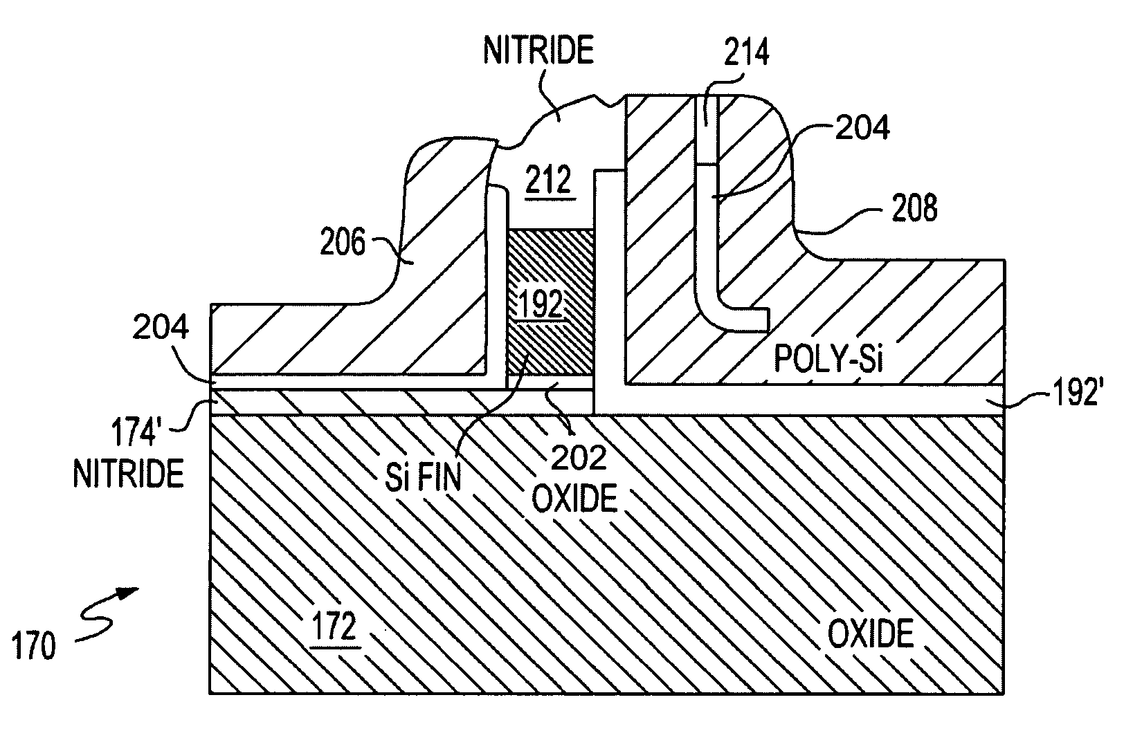
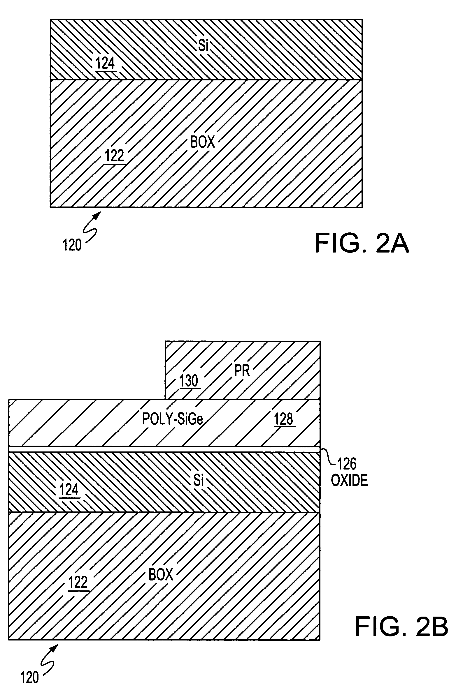
[0017]Turning now to the drawings and, more particularly, FIG. 1 shows an example of a preferred embodiment method for forming dual gate field effect transistors (FETs), e.g., in an integrated circuit (IC) and, more particularly FinFETs, according to the present invention. Further, one gate of preferred embodiment dual gate FinFETs may be used to adjust the thresholds for the other, i.e., operating to effectively back bias the device for the other, normal device gate. So, circuit / device formation begins in step 102 with a typical semiconductor wafer preferably, a silicon on insulator (SOI) wafer. Then in step 104 device fins are defined and in step 106 formed from an upper surface semiconductor layer, e.g., a silicon layer. Then, in step 108, a back bias gate is formed along a back side of the device fins. In step 110 a conductive gate layer is formed over the wafer including over device fins and back bias gates. In step 112, the gate layer is patterned to define gates, i.e., divide...


PUM


Abstract

A field effect transistor (FET), integrated circuit (IC) chip including the FETs and a method of forming the FETS. Each FET includes a device gate along one side of a semiconductor (e.g., silicon) fin and a back bias gate along an opposite of the fin. Back bias gate dielectric differs from the device gate dielectric either in its material and / or thickness. Device thresholds can be adjusted by adjusting back bias gate voltage.

Description

BACKGROUND OF THE INVENTION[0001]1. Field of the Invention[0002]The present invention is related to semiconductor devices and manufacturing and more particularly to field effect transistors (FETs) formed on silicon on insulator (SOI) wafers and methods of manufacturing FETs and circuits on SOI wafers.[0003]2. Background Description[0004]Semiconductor technology and chip manufacturing advances have resulted in a steady increase of on-chip clock frequencies, the number of transistors on a single chip and the die size itself, coupled with a corresponding decrease in chip supply voltage and chip feature size. Generally, all other factors being constant, the power consumed by a given clocked unit increases linearly with the frequency of switching within it. Thus, not withstanding the decrease of chip supply voltage, chip power consumption has increased as well. Both at the chip and system levels, cooling and packaging costs have escalated as a natural result of this increase in chip powe...

Claims


Application Information

Patent Timeline
Patent Type & Authority Patents(United States)
IPC IPC(8): H01L29/76H01L29/94H01L31/062H01L31/113H01L31/119H01L21/336H01L21/84H01L27/01H01L27/12H01L29/78H01L29/786
CPCH01L29/785H01L29/66795H01L29/7856
Inventor ZHU, HUILONGBEINTNER, JOCHENDORIS, BRUCE B.ZHANG, YING
Owner GLOBALFOUNDRIES US INC
Why Eureka
Try Eureka