
Open pattern inductor

a technology of open pattern and inductor, which is applied in the manufacture of inductances/transformers/magnets, waveguide devices, inductances, etc., can solve the problems of inability to precisely and inexpensively fabricate helical structures with cores, and the conventional integrated circuit process steps do not lend themselves to precisely and inexpensively fabricating helical structures. the effect of inductan

Inactive Publication Date: 2006-08-15
MICRON TECH INC
View PDF27 Cites 20 Cited by
  • Summary
  • Abstract
  • Description
  • Claims
  • Application Information

AI Technical Summary

Benefits of technology

This approach enables the creation of high-inductance inductors without increasing surface area, reducing power consumption and noise, while being compatible with silicon integrated circuit processes, thus addressing the need for miniaturized and cost-effective inductors.

Problems solved by technology

Active inductors can be designed to have a high inductance and a high Q factor, but inductors fabricated using these designs consume a great deal of power and generate noise.
Unfortunately, conventional integrated circuit process steps do not lend themselves to precisely and inexpensively fabricating a helical structure with a core.
So, integrated circuit process technology is only marginally compatible with manufacturing a solenoid type inductor.
Unfortunately, this approach has a high cost factor associated with it when applied to fabricating inductors for use in silicon integrated circuits.

Method used


Image

  • Open pattern inductor
  • Open pattern inductor
  • Open pattern inductor

Examples


Embodiment Construction

[0021]In the following detailed description, reference is made to the accompanying drawings which form a part hereof, and in which is shown by way of illustration specific embodiments in which the invention may be practiced. These embodiments are described in sufficient detail to enable those skilled in the art to practice the invention, and it is to be understood that other embodiments may be utilized and that structural, logical and electrical changes may be made without departing from the spirit and scope of the present invention. The following detailed description is, therefore, not to be taken in a limiting sense, and the scope of the present invention is defined by the appended claims.

[0022]Inductors intended for use in circuits fabricated on a silicon substrate usually operate at lower frequencies and require larger inductances than inductors intended for use in circuits fabricated on a gallium arsenide substrate. As mentioned above, a larger inductance is usually realized in...


PUM

PropertyMeasurementUnit
non-magneticaaaaaaaaaa
magneticaaaaaaaaaa
permeabilityaaaaaaaaaa

Abstract

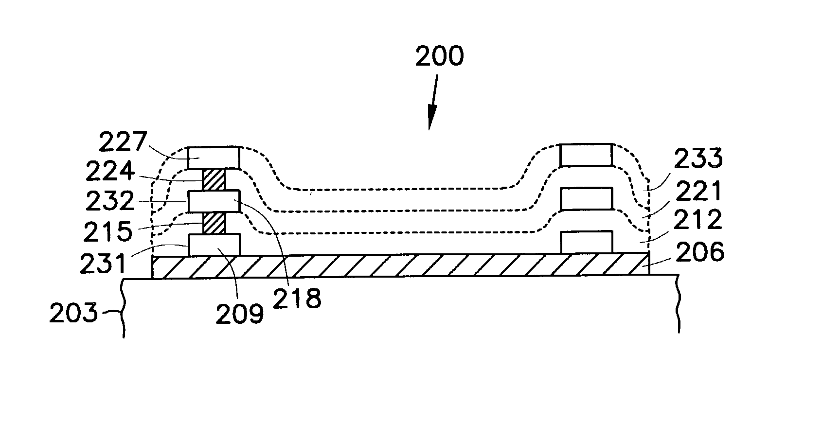
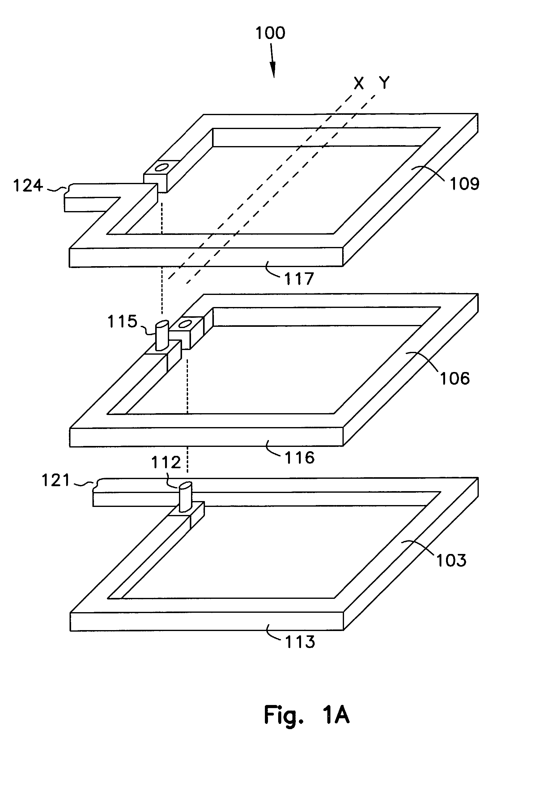
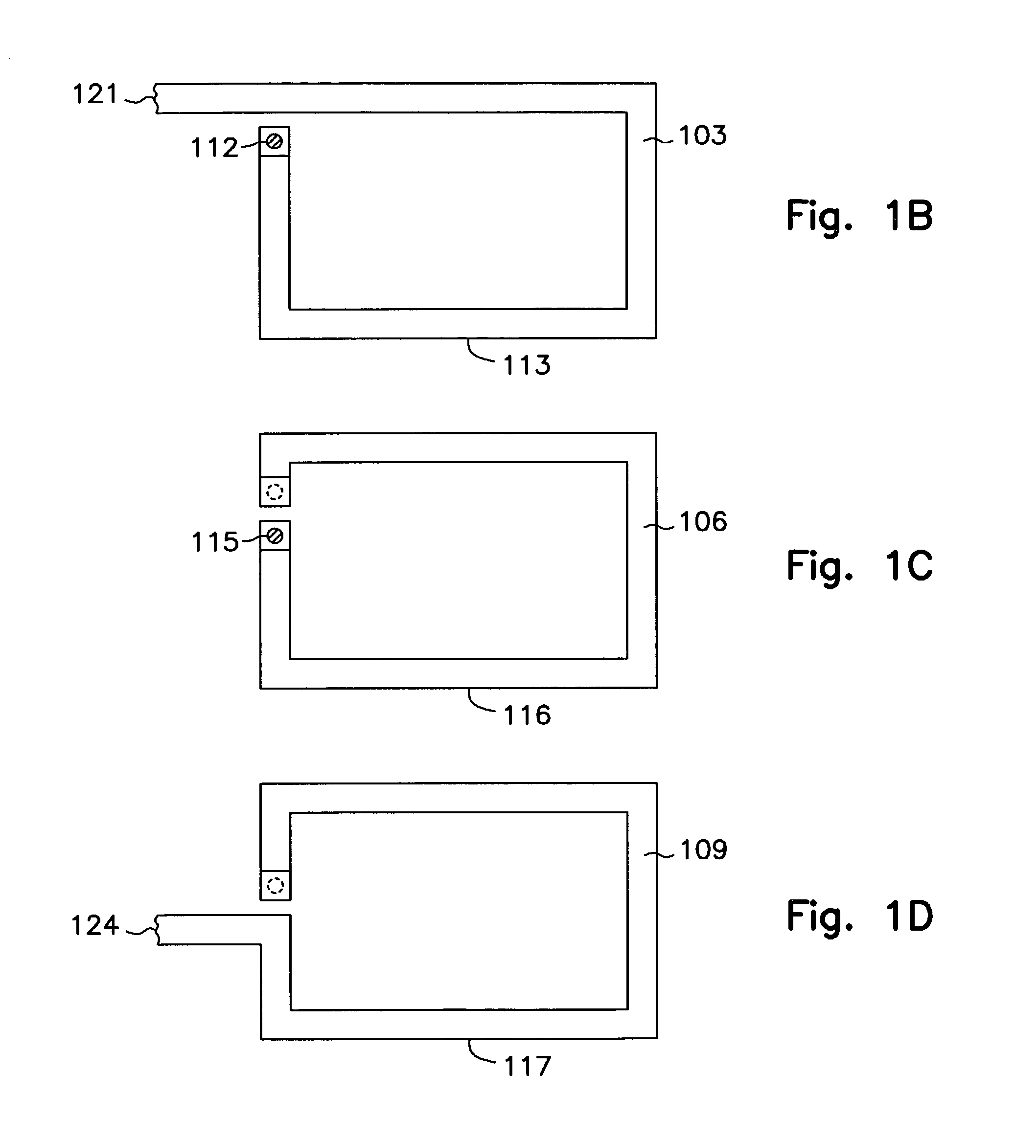
The invention includes a stacked open pattern inductor fabricated above a semiconductor substrate. The stacked open pattern inductor includes a plurality of parallel open conducting patterns embedded in a magnetic oxide or in an insulator and a magnetic material. Embedding the stacked open pattern inductor in a magnetic oxide or in an insulator and a magnetic material increases the inductance of the inductor and allows the magnetic flux to be confined to the area of the inductor. A layer of magnetic material may be located above the inductor and below the inductor to confine electronic noise generated in the stacked open pattern inductor to the area occupied by the inductor. The stacked open pattern inductor may be fabricated using conventional integrated circuit manufacturing processes, and the inductor may be used in connection with computer systems.

Description

RELATED APPLICATIONS[0001]This application is a divisional of U.S. application Ser. No. 09 / 261,595 filed on Feb. 26, 1999, now U.S. Pat. No. 6,566,731, the specification of which is incorporated herein by reference.FIELD OF THE INVENTION[0002]The present invention relates to inductors, and more particularly, to inductors used in integrated circuits.BACKGROUND OF THE INVENTION[0003]The telecommunications and computer industries are driving the demand for miniaturized analog and mixed signal circuits. Inductors are a critical component in the traditional discrete element circuits, such as impedence matching circuits, resonant tank circuits, linear filters, and power circuits, used in these industries. Since traditional inductors are bulky components, successful integration of the traditional discrete element circuits requires the development of miniaturized inductors.[0004]One approach to miniaturizing an inductor is to use standard integrated circuit building blocks, such as resistor...

Claims


Application Information

Patent Timeline
Patent Type & Authority Patents(United States)
IPC IPC(8): H01L29/00H01F5/00H01F17/00H01F27/36H01F41/04H01L21/02H01L27/08H10N97/00
CPCH01F17/0013H01F41/046H01L27/08Y10T29/49075Y10T29/49073Y10T29/49071Y10T29/49069Y10T29/4902Y10T29/49062Y10T29/4906H01L28/10H01F27/36H01P11/007H01F41/043H01P9/02
Inventor AHN, KIE Y.FORBES, LEONARD
Owner MICRON TECH INC
Learn More