Liquid crystal display device and method for fabricating thereof

a liquid crystal display and liquid crystal technology, applied in non-linear optics, instruments, optics, etc., can solve problems such as the allowable limi

Inactive Publication Date: 2006-08-22
SEMICON ENERGY LAB CO LTD
View PDF48 Cites 13 Cited by
  • Summary
  • Abstract
  • Description
  • Claims
  • Application Information

AI Technical Summary

Problems solved by technology

Also, they conceived that there is an allowable limit also in respect of the stepped difference which gives rise to the alignment defect in the rubbing operation.

Method used


Image

  • Liquid crystal display device and method for fabricating thereof
  • Liquid crystal display device and method for fabricating thereof
  • Liquid crystal display device and method for fabricating thereof

Examples


embodiment 1

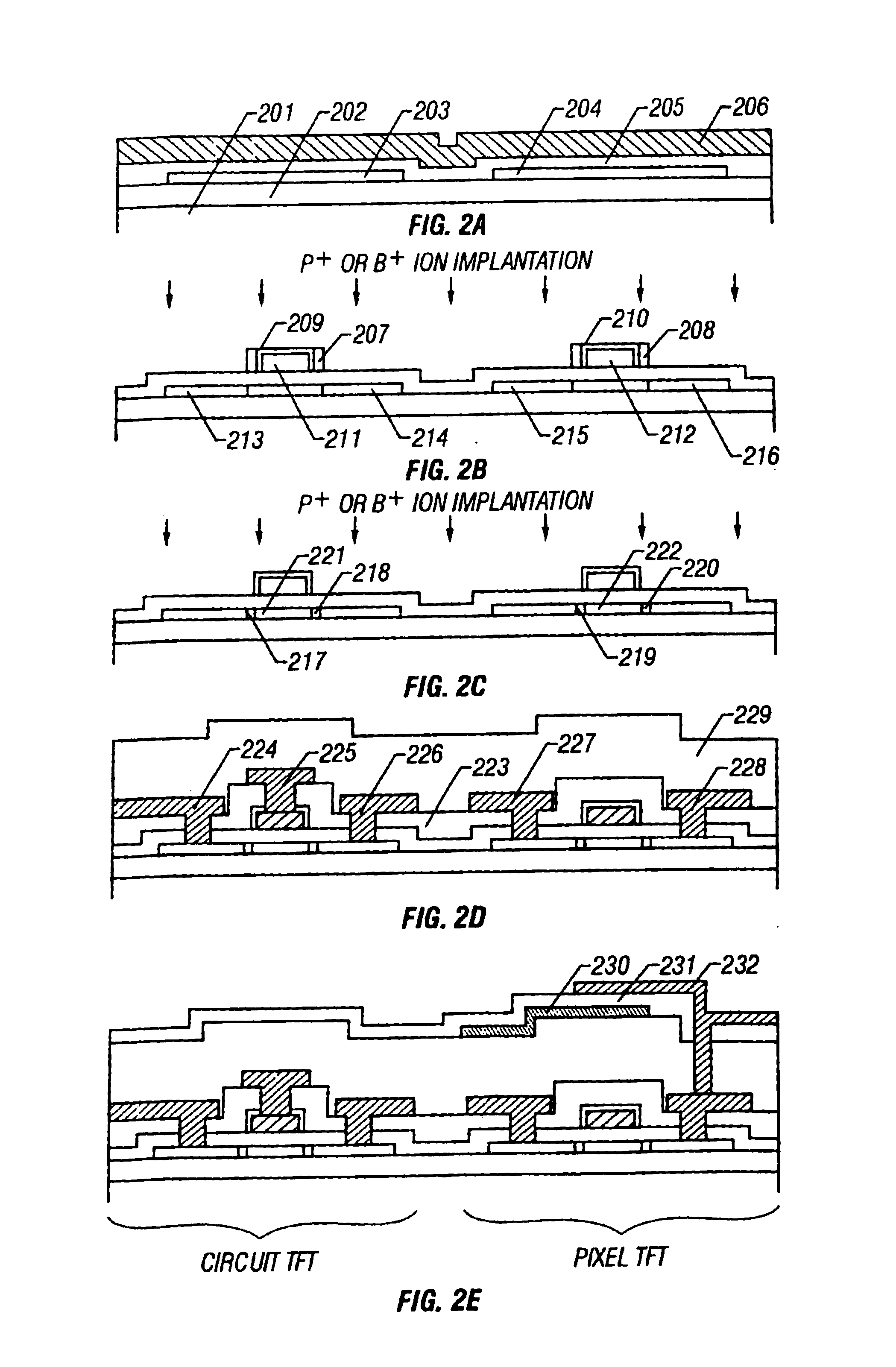
[0049]With respect to Embodiment 1 an explanation will be given of details of steps of fabricating a liquid crystal display device based on the present invention. An explanation will be given of fabrication steps of a circuit TFT (Thin Film Transistor) and a pixel TFT arranged on an active matrix substrate in reference to FIGS. 2(A), 2(B), 2(C), 2(D) and 2(E) and an explanation will be given of fabrication steps (cell integration steps) of the liquid crystal display device in reference to FIGS. 3(A), 3(B), 3(C) and 3(D).

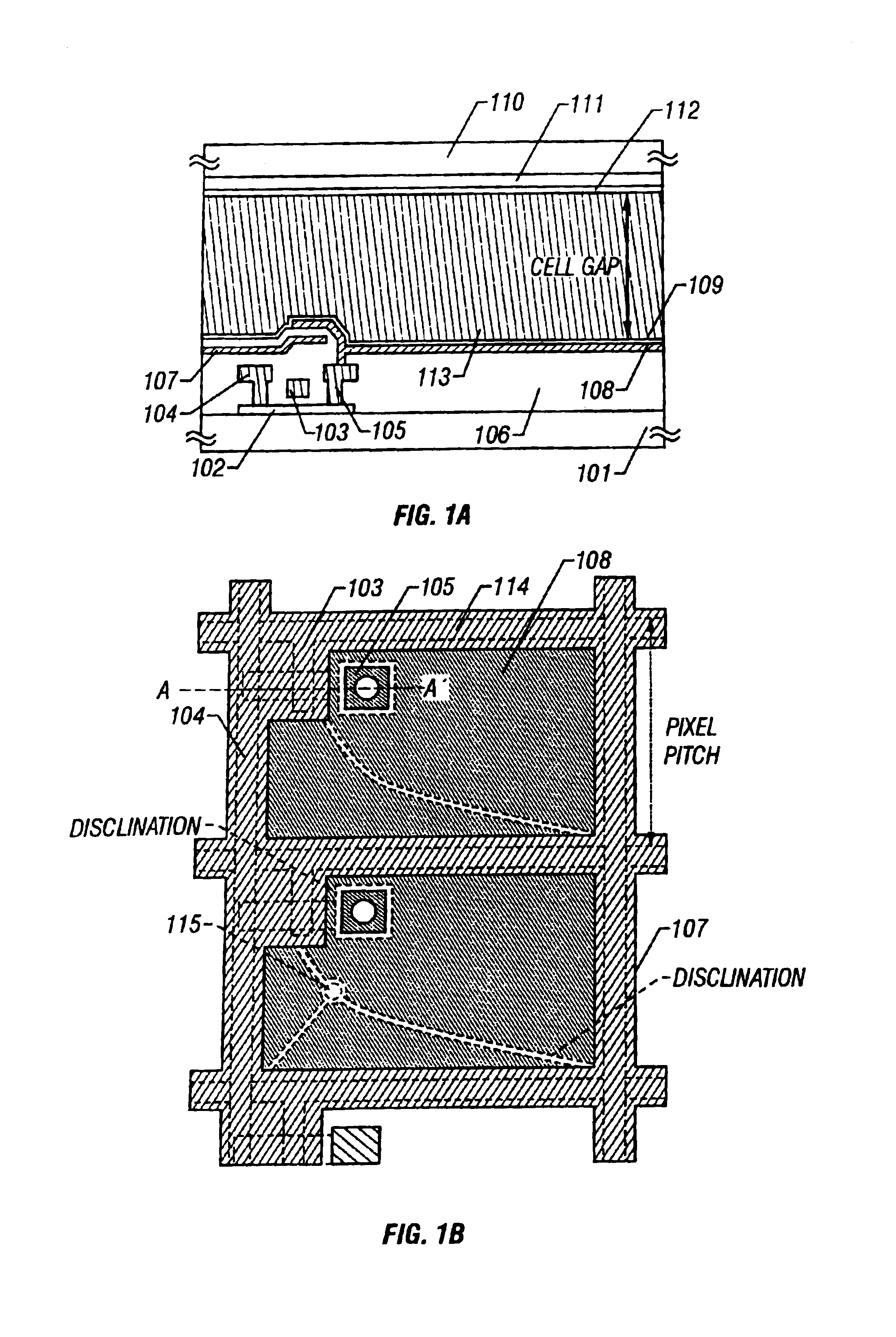
[0050]Incidentally, Embodiment 1 will be described by paying attention to mainly the correlation between the pixel pitch and the cell gap. Therefore, in Embodiment 1 the stepped difference stays at a nonproblematic level of 0.3 μm or less and an explanation thereof will not be given.

[0051]Firstly, a substrate having insulating performance, for example, a glass substrate 201 represented by Corning 7059 or Corning 1737 or the like is prepared. A silicon oxide film is f...

embodiment 2

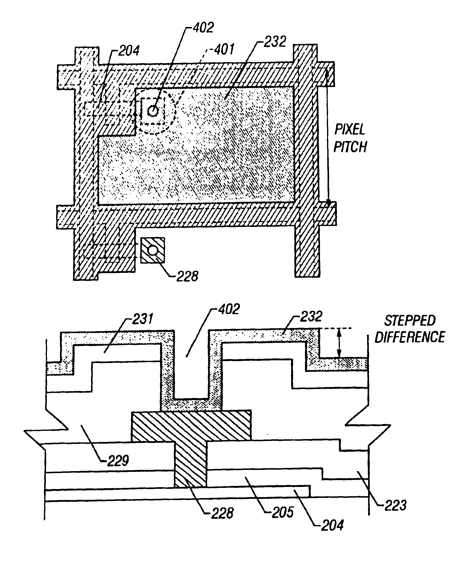
[0104]An explanation will be given of Embodiment 2 by paying attention to a stepped difference in accordance with the present invention. In Embodiment 2, an example of an active matrix type liquid crystal display device using a thin film transistor having the constitution where a pixel electrode is connected to a drain electrode that is connected to an active layer.

[0105]As mentioned above, the stepped differences are formed at the surroundings of the thin film transistor and the respective wirings, and may cause alignment defect of a liquid crystal material by causing rubbing failure or creating a horizontal electric field generated at side faces of the stepped differences.

[0106]Normally, even if a disclination caused by the stepped difference of a wiring intersecting portion or on a thin film transistor occurs, the disclination poses no problem since it can be hidden by a black matrix. Also, in the case where the black matrix is installed on the side of the opposed substrate the p...


PUM

PropertyMeasurementUnit
thicknessaaaaaaaaaa
circumferenceaaaaaaaaaa
thicknessesaaaaaaaaaa

Abstract

To provide a technology for fabricating a high image quality liquid crystal display device, a set range of a cell gap for holding a liquid crystal layer is limited in accordance with a distance of a pixel pitch in which specifically, the cell gap is set to be a distance of one tenth of the pixel pitch, whereby the high image quality liquid crystal display device with no occurrence of image display failure caused by disturbances of an electric field such as disclination, can be realized.

Description

[0001]This is a continuation of application Ser. No. 08 / 835,725, filed Apr. 11, 1997, now U.S. Pat. No. 6,323,932.BACKGROUND OF THE INVENTION[0002]1. Field of the Invention[0003]The present invention disclosed in the specification relates to a liquid crystal display device having pixel areas arranged in a matrix form on a same substrate, particularly to an active matrix type liquid crystal display device having semiconductor devices using semiconductor thin films. Silicon films can representatively be used as the semiconductor thin films.[0004]2. Description of Related Art[0005]In recent times, technologies for making a semiconductor device using semiconductor thin films, for example, a thin film transistor (TFT) on an inexpensive glass substrate have been rapidly developed. The reason is that demand for an active matrix type liquid crystal display device has been enhanced.[0006]According to an active matrix type liquid crystal display device, TFTs are arranged to each of pixel area...

Claims


Application Information

Patent Timeline
Patent Type & Authority Patents(United States)
IPC IPC(8): G02F1/1339G02F1/136G02F1/1362G02F1/1368
CPCG02F1/13392G02F1/136209G02F1/1362G02F1/1341G02F2001/133388G02F1/136227G02F1/133388G02F1/136
Inventor ZHANG, HONGYONGFUKUNAGA, TAKESHI
Owner SEMICON ENERGY LAB CO LTD
Why Eureka
Try Eureka