Exposure method and apparatus

a technology of exposure method and apparatus, applied in the field of exposure, can solve the problems of increasing mask manufacturing cost, difficult to make the residual aberration small, complex mask design, etc., and achieve the effect of reducing image quality degradation and good resolution

Inactive Publication Date: 2006-08-22
CANON KK
View PDF7 Cites 26 Cited by
  • Summary
  • Abstract
  • Description
  • Claims
  • Application Information

AI Technical Summary

Benefits of technology

[0012]Accordingly, it is an exemplary object of the present invention to provide an exposure method and apparatus with good resolution, w

Problems solved by technology

However, a short wavelength of exposure light and a high NA of a projection optical system make it difficult to make the residual aberration small.
However, this requires an appropriate size offset and an auxiliary pattern shape to be determined for each exposure according to a residual aberration in a projection optical system and shape changes in a circuit pattern, making a mask design complex.
In addition, additions of a size offset and an auxiliary pa

Method used


Image

  • Exposure method and apparatus
  • Exposure method and apparatus
  • Exposure method and apparatus

Examples


Embodiment Construction

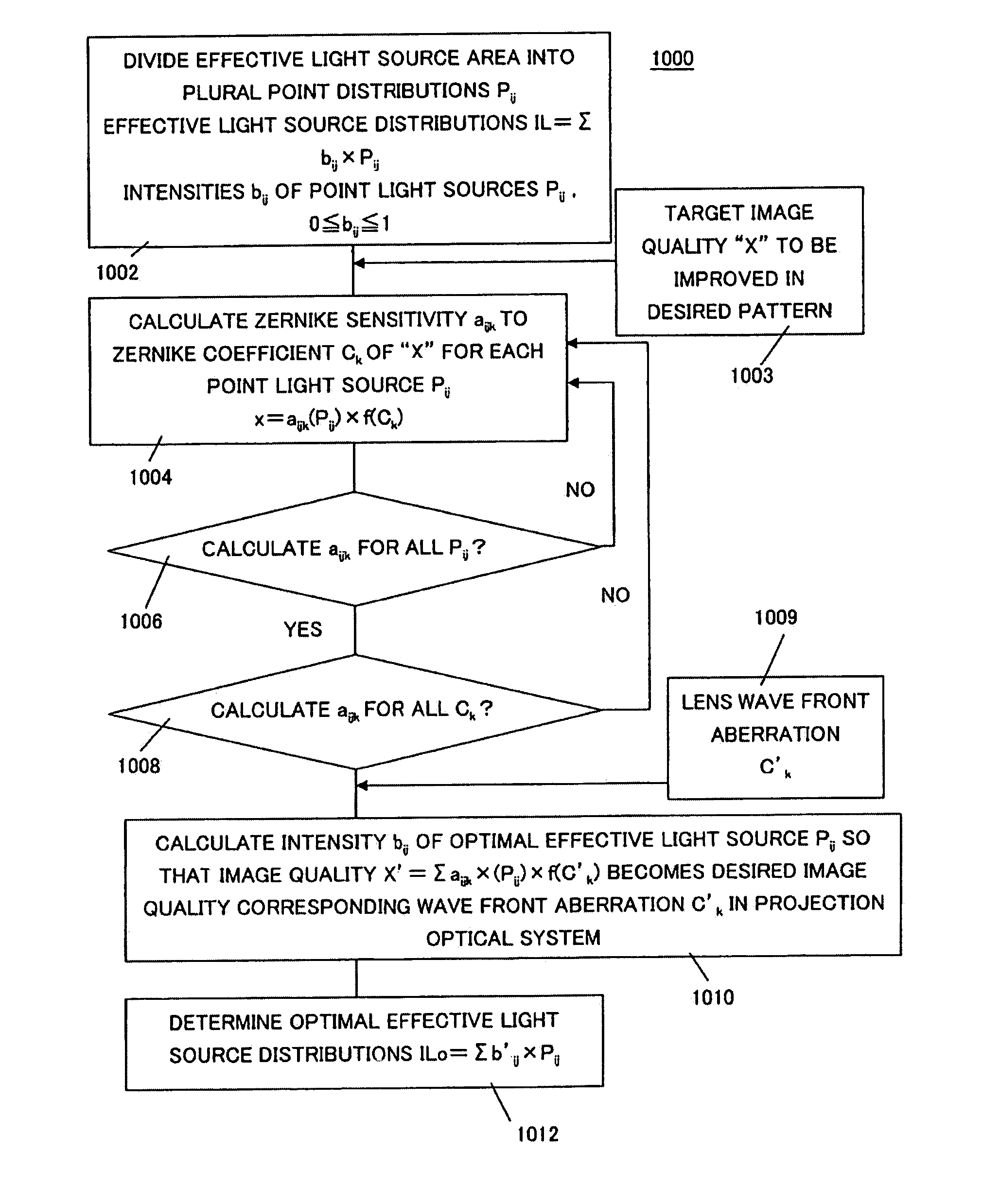
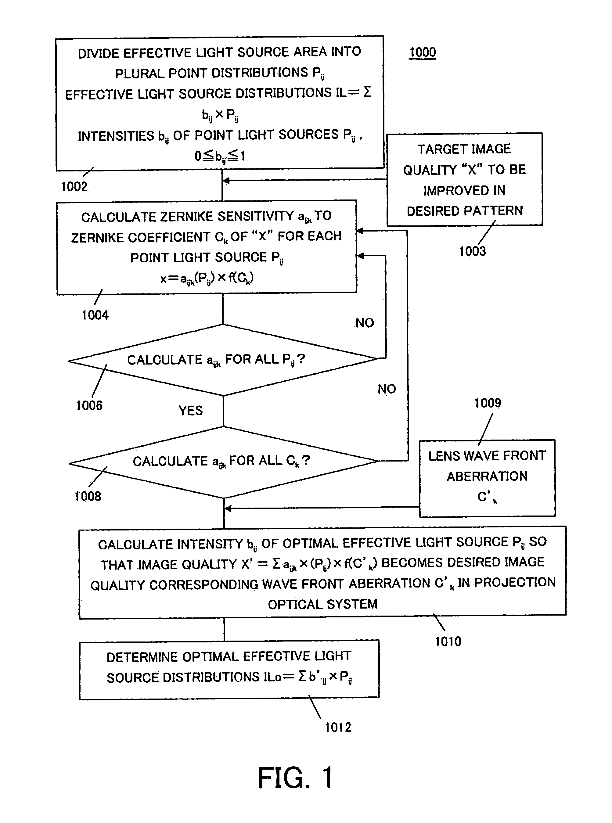
[0041]With reference to the accompanying drawings, a description will now be given of an exposure method and apparatus according to the present invention. In each figure, the same element is designated by the same reference numeral, and a description thereof will be omitted.

[0042]FIG. 1 is a flowchart for explaining an exposure method 1000 of one embodiment according to the present invention. The exposure method 1000 projects, through a projection optical system, a desired pattern formed on a mask onto an object to be exposed.

[0043]Referring now to FIG. 1, an effective light source area for illuminating the mask is divided into plural point light sources (step 1002). For example, the effective light source is divided like a lattice and expressed by a suffix of a row number i and a column number j, i.e., like a point light source Pij at a position having a row number i and a column number j. Equation 3 below represents an arbitrary effective light source distribution IL in the effect...


PUM


Abstract

An exposure method for projecting, through a projection optical system, a predetermined pattern formed on a mask onto an object to be exposed. The exposure method includes the steps of dividing an effective light source area for illuminating the mask into plural point light sources, calculating a Zernike sensitivity coefficient that represents a sensitivity of a change of image quality of the predetermined pattern to a change of a Zernike coefficient, when wave front aberration in the projection optical system is developed into a Zernike polynomial for all divided point light sources, determining an effective light source distribution based on a combination of Zernike sensitivity coefficient of all divided point light sources, and forming the effective light source distribution by intensity of each point light source.

Description

BACKGROUND OF THE INVENTION[0001]The present invention generally relates to exposure, and, more particularly, to an exposure method and apparatus for fabricating various types of devices such as semiconductor chips, such as ICs and LSIs, display devices, such as liquid crystal panels, a detection device, such as thin film magnetic heads, and image pickup devices, such as CCDs.[0002]In manufacturing fine semiconductor devices such as a semiconductor memory and a logic circuit in photolithography technology, a reduction projection exposure apparatus has been conventionally employed, which uses a projection optical system to project a circuit pattern formed on a mask (reticle) onto a wafer, etc., to transfer the circuit pattern.[0003]Recent demands for smaller and finer electronic apparatuses have increasingly called for fine processing to semiconductor devices mounted onto the electronic apparatuses. The critical dimension transferable by the projection exposure apparatus or resolutio...

Claims


Application Information

Patent Timeline
IPC IPC(8): G03B27/68G03B27/32G03B27/42G03F7/20H01L21/027
CPCG03F7/706G03F7/70133
Inventor MOROHOSHI, HIROSHI
Owner CANON KK
Why Eureka
Try Eureka