

Measurement of optical properties of radiation sensitive materials
a radiation sensitive material and optical property technology, applied in semiconductor/solid-state device testing/measurement, phase-affecting property measurement, instruments, etc., can solve the problems of chemical and/or physical changes of materials, and achieve the effect of accurate measurement of radiation sensitive film optical properties and lower signal-to-noise ratio
- Summary
- Abstract
- Description
- Claims
- Application Information
AI Technical Summary
Benefits of technology
Problems solved by technology
Method used
Image

Examples
Embodiment Construction
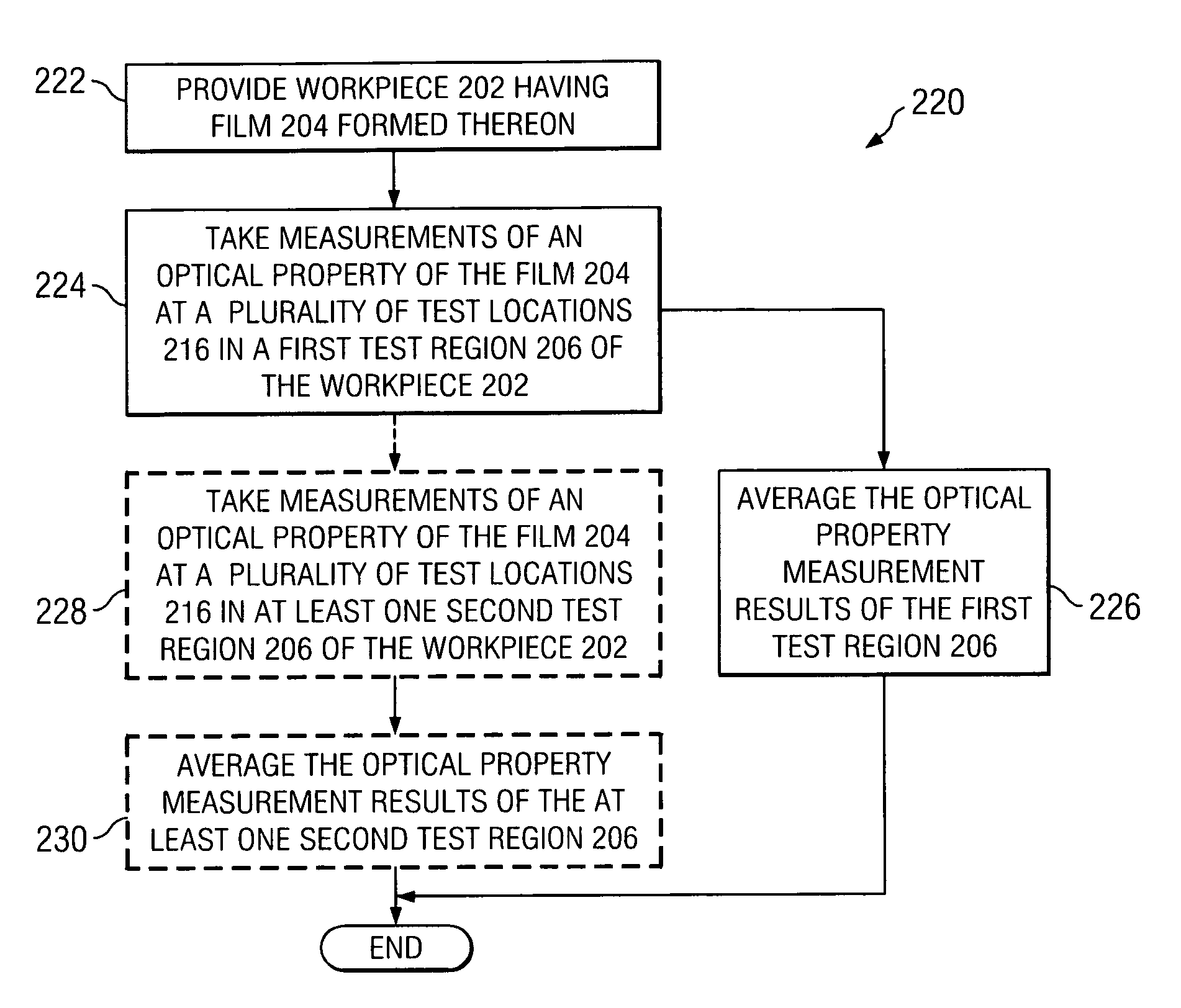
[0028]The making and using of the presently preferred embodiments are discussed in detail below. It should be appreciated, however, that the present invention provides many applicable inventive concepts that can be embodied in a wide variety of specific contexts. The specific embodiments discussed are merely illustrative of specific ways to make and use the invention, and do not limit the scope of the invention.
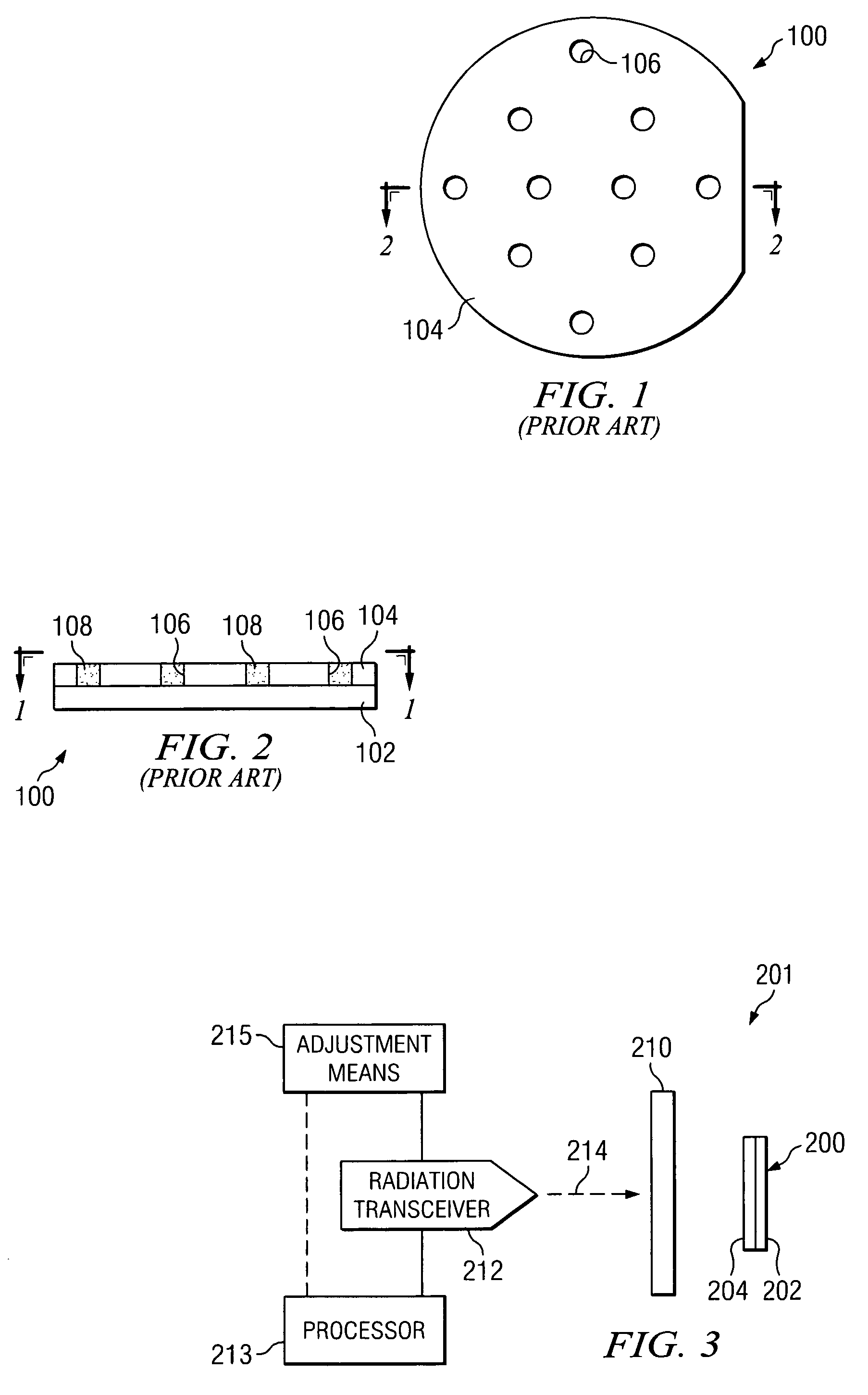
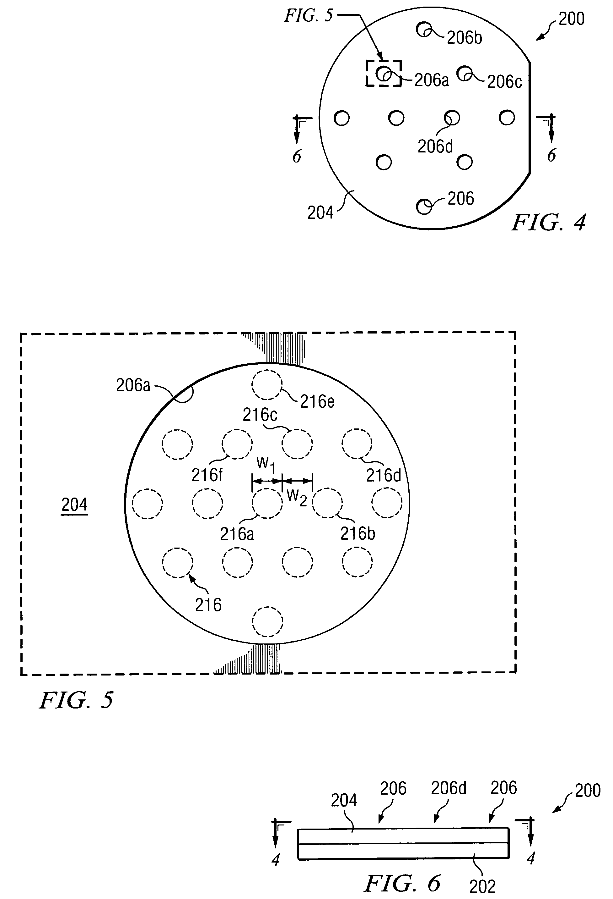
[0029]The present invention will be described with respect to preferred embodiments in a specific context, namely, a semiconductor wafer or workpiece. The invention may also be applied, however, to films deposited or formed on other objects, for example. Embodiments of the present invention are preferably used to measure optical properties of labile or radiation sensitive materials, although embodiments of the present invention also have application in the measurements of optical properties of stable or radiation insensitive materials.
[0030]The refractive index is an optical ...
PUM
| Property | Measurement | Unit |
|---|---|---|
| wavelengths | aaaaa | aaaaa |
| wavelengths | aaaaa | aaaaa |
| thickness | aaaaa | aaaaa |
Abstract
Description
Claims
Application Information