

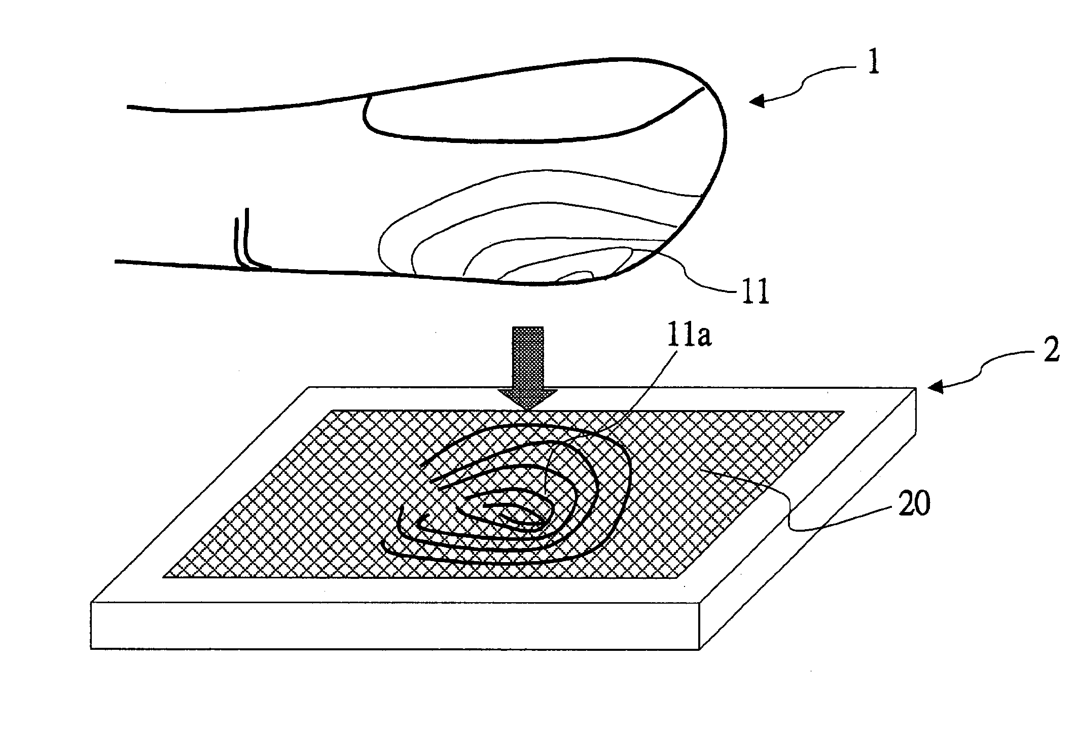
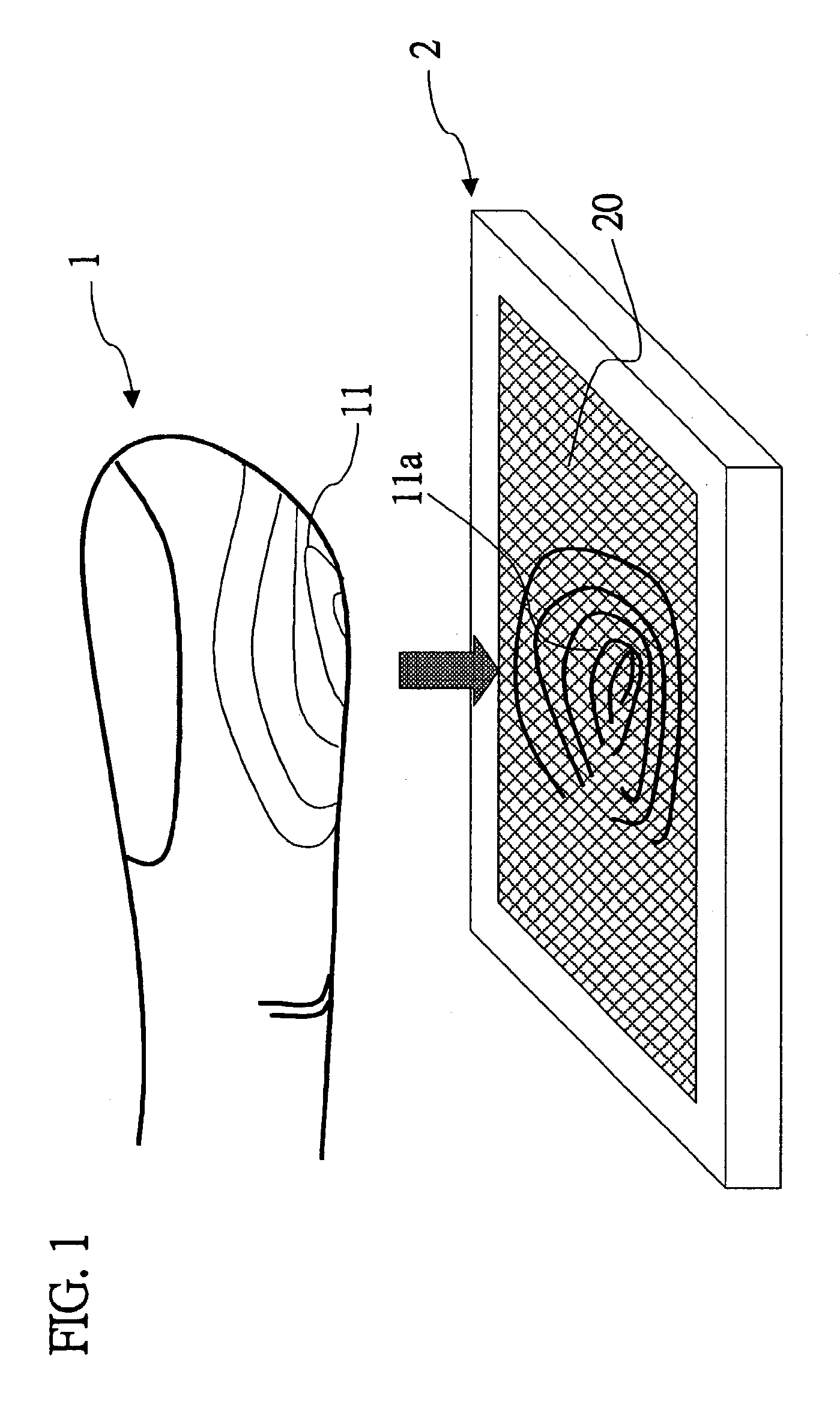
Capacitive fingerprint sensor
a fingerprint sensor and capacitive technology, applied in the field of capacitive fingerprint sensors, can solve the problems of disadvantageous large size of fingerprint sensors utilizing the methods, inability to meet the requirement of real-time authentication, and inability to process fingerprint identification in real-time, so as to achieve the effect of cleaning residual charges
- Summary
- Abstract
- Description
- Claims
- Application Information
AI Technical Summary
Benefits of technology
Problems solved by technology
Method used
Image

Examples
Embodiment Construction
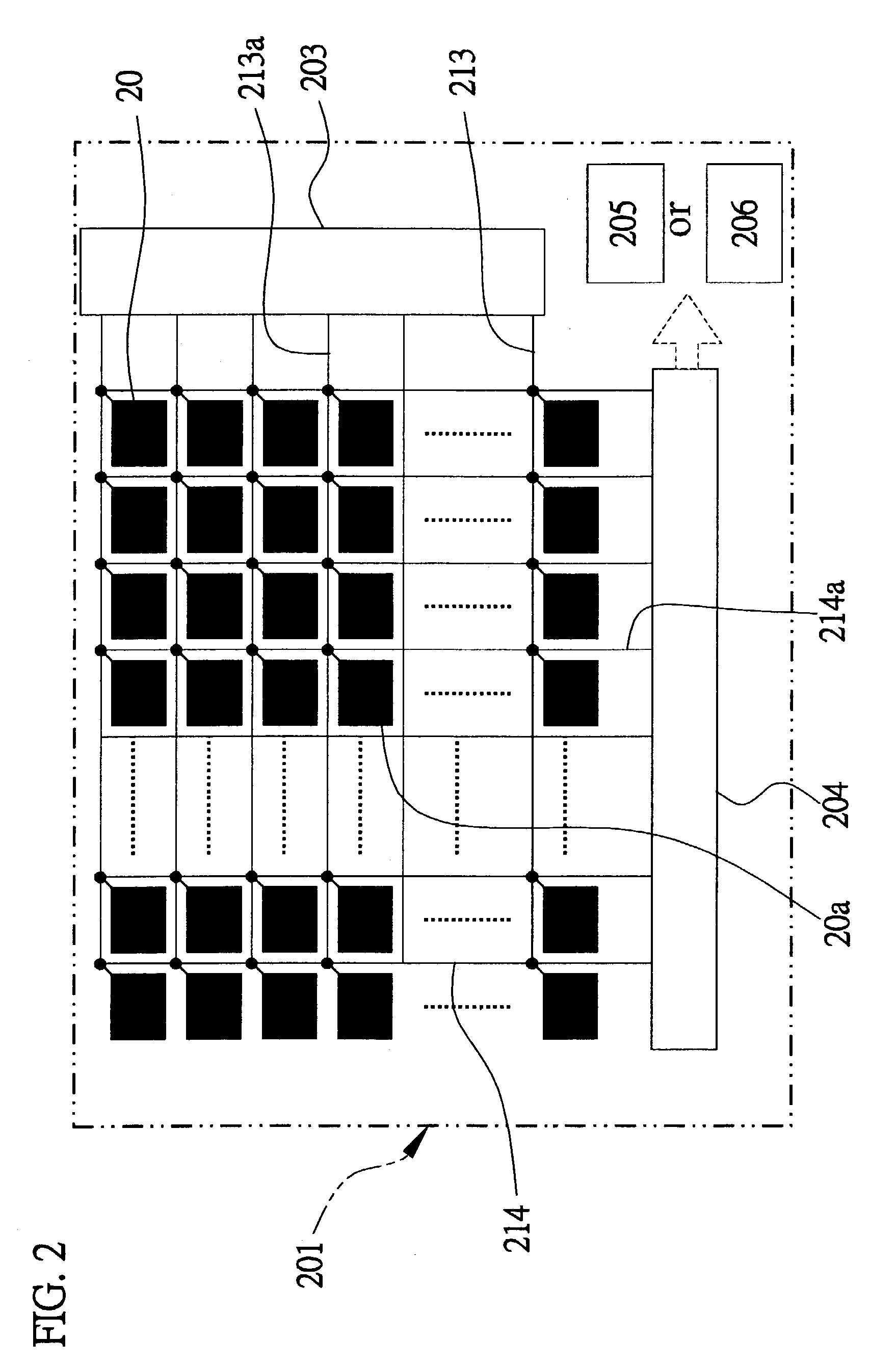
[0019]Unlike the designs of reading circuits in other capacitive fingerprint sensors, the invention utilizes a charge-sharing principle to read the capacitance. The principle basically comes from the design of a dynamic random access memory (DRAM) except for the difference residing in that the DRAM utilizes wire's parasitic capacitor as a reference capacitor and the output of the DRAM is binary output (0 or 1). Instead, the invention utilizes a specific reference capacitor, and the ratios of each reference capacitance to a corresponding sense capacitance are precisely controlled. Hence, even if there are errors in manufacturing the sensing members, good image uniformity may be obtained as long as the ratios of each sense capacitance to each corresponding reference capacitance of the sensing members in a local area can be kept the same. The effect can be obtained according to the actual IC manufacturing technology. Furthermore, the circuit architecture for implementing the charge-sha...
PUM
 Abstract
Description
Claims
Application Information