Reflective mask for short wavelength lithography

Active Publication Date: 2006-09-05
ADVANCED MICRO DEVICES INC +1
View PDF10 Cites 11 Cited by
  • Summary
  • Abstract
  • Description
  • Claims
  • Application Information

AI Technical Summary

Benefits of technology

[0010]According to one or more aspects of the present invention, a reflective mask, for example, an extreme ultraviolet (EUV) reflective mask, that can be utilized to transfer a pattern onto a wafer during a semiconductor fabrication process includes a patterned reflective coating and a substrate over which the reflective coating is formed. The substrate is absorbent to radiation (e.g., EUV radiation) such that radiation incident to the substrate is not reflected substantially therefrom, and the circuit design patterned within the reflective coating is transferred. In one example, the mask does not include other radiation absorbent material (e.g., EUV absorbent material), other than the substrate, and this lack of other absorbent material mitigates the occurrence and severity of dead zones, which commonly occur in conventional masks and which degrade the fidelity of pattern transfers.
[0011]In accordance with one or more other aspects of the present invention, a methodology for fabricating a reflective mask includes patterning a masking material, such as a photoresist, and a reflective coating with the patterned masking material serving as a mask for the reflective coating. The reflective coating overlies an absorbent substrate, and as such, ther

Problems solved by technology

However, as feature sizes continue to decrease, optical systems are approaching

Method used


Image

  • Reflective mask for short wavelength lithography
  • Reflective mask for short wavelength lithography
  • Reflective mask for short wavelength lithography

Examples


Embodiment Construction

[0022]One or more aspects of the present invention arc described with reference to the drawings, wherein like reference numerals are generally utilized to refer to like elements throughout, and wherein the various structures are not necessarily drawn to scale. In the following description, for purposes of explanation, numerous specific details are set forth in order to provide a thorough understanding of one or more aspects of the present invention. It may be evident, however, to one skilled in the art that one or more aspects of the present invention may be practiced with a lesser degree of these specific details. In other instances, well-known structures and devices are shown in block diagram form in order to facilitate describing one or more aspects of the present invention.

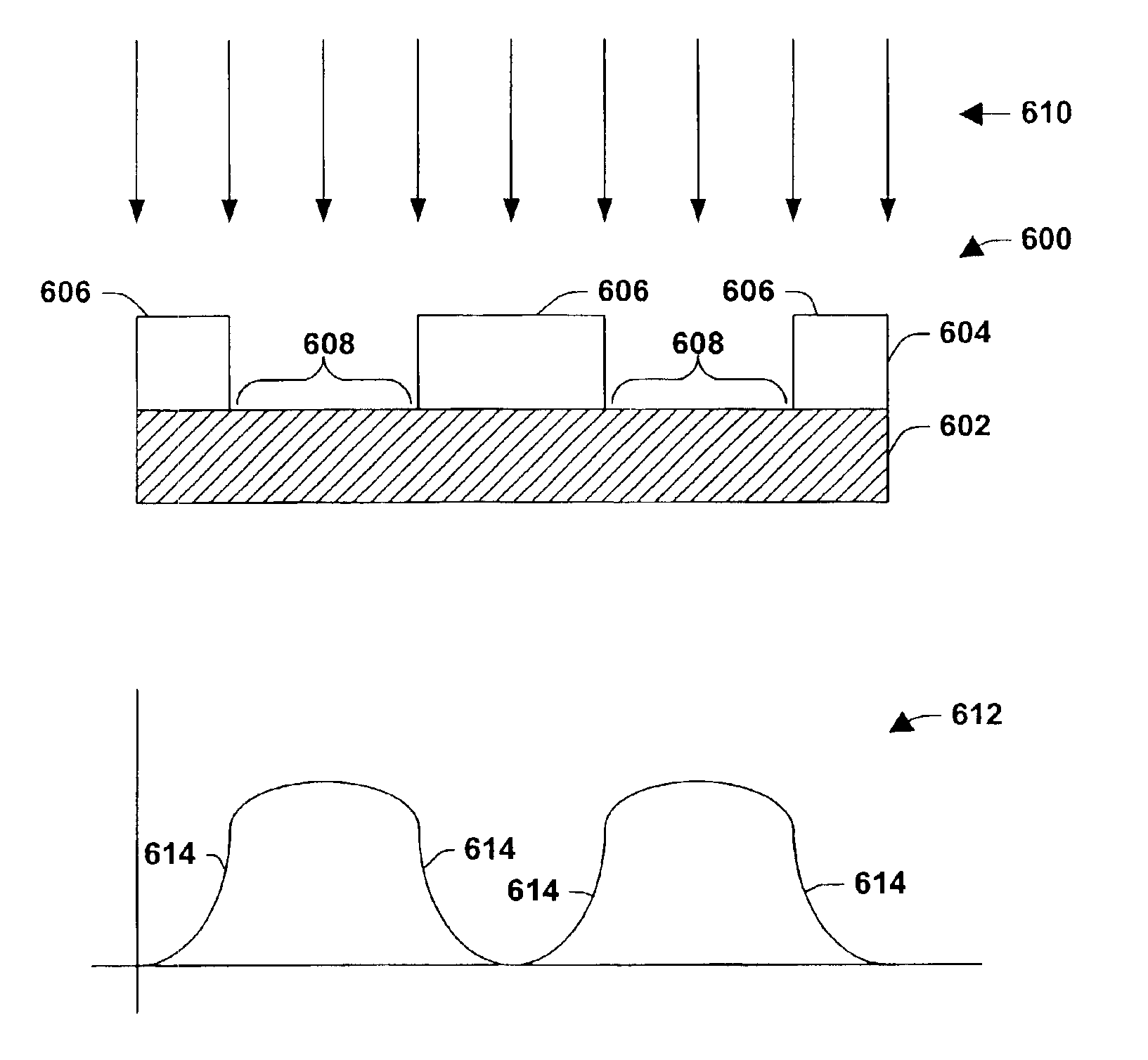
[0023]One or more aspects of the present invention relate to a reflective mask that can be utilized to transfer a pattern onto a wafer during a semiconductor fabrication process, as well as to a methodology fo...


PUM


Abstract

A reflective mask (e.g., an EUV reflective mask) and a method of making such a mask are disclosed. The mask includes an absorbent substrate and a reflective coating overlying the substrate. The reflective coating is patterned to include a circuit design that is to be transferred onto one or more wafers, and more particularly onto one or more die on the wafers, during semiconductor fabrication processing. The mask includes no other radiation absorbent material, and the occurrence and severity of dead zones, which commonly occur in conventional reflective masks and which degrade the fidelity of pattern transfers, are thereby mitigated. A methodology for inspecting the mask via the transmission of visible, UV or deep-UV radiation through the mask is also disclosed.

Description

FIELD OF INVENTION[0001]The present invention relates generally to a reflective mask for use in lithography such as extreme-UV (EUV) lithography.BACKGROUND OF THE INVENTION[0002]In the semiconductor industry, there is a continuing trend toward higher device densities. To achieve these high densities there has been, and continues to be, efforts toward scaling down the device dimensions on semiconductor wafers. In order to accomplish such a high device packing density, smaller features sizes are required. This may include the width and spacing of interconnecting lines and the surface geometry such as the corners and edges of various features.[0003]The requirement of small features with close spacing between adjacent features requires high resolution photolithographic processes. In general, lithography refers to processes for pattern transfer between various media. With regard to semiconductor fabrication, a silicon slice (e.g., a wafer) is coated uniformly with a radiation-sensitive f...

Claims


Application Information

Patent Timeline
IPC IPC(8): G03F9/00G21K5/00
CPCB82Y10/00B82Y40/00G21K1/062G03F1/84G03F1/24
Inventor LA FONTAINE, BRUNODIEU, LAURENT
Owner ADVANCED MICRO DEVICES INC
Why Eureka
Try Eureka