Dual double gate transistor and method for forming

a technology of double gate transistor and field effect, which is applied in the direction of transistors, semiconductor devices, electrical equipment, etc., can solve the problems of reducing the performance and/or reliability, and affecting the design and fabrication of dual gate transistors. achieve the effect of improving device performance and density, and improving current control over traditional dual gate designs

Inactive Publication Date: 2006-09-05
GLOBALFOUNDRIES US INC
View PDF13 Cites 28 Cited by
  • Summary
  • Abstract
  • Description
  • Claims
  • Application Information

AI Technical Summary

Benefits of technology

[0011]Accordingly, the present invention provides a dual gate transistor and a method for forming the same that results in improved device performance and density. The present invention uses a double gate design to implement a dual gate transistor. A double gate is a gate which is formed on both sides of the transistor body. The present invention thus provides a

Problems solved by technology

FETs are used in almost all types of integrated circuit design (i.e., microprocessors, memory, etc.) Unfortunately, increased device density in CMOS FET can result in degradation of performance and/or reliability.
Unfortunately, several difficulties arise in the design and

Method used


Image

  • Dual double gate transistor and method for forming
  • Dual double gate transistor and method for forming
  • Dual double gate transistor and method for forming

Examples


Embodiment Construction

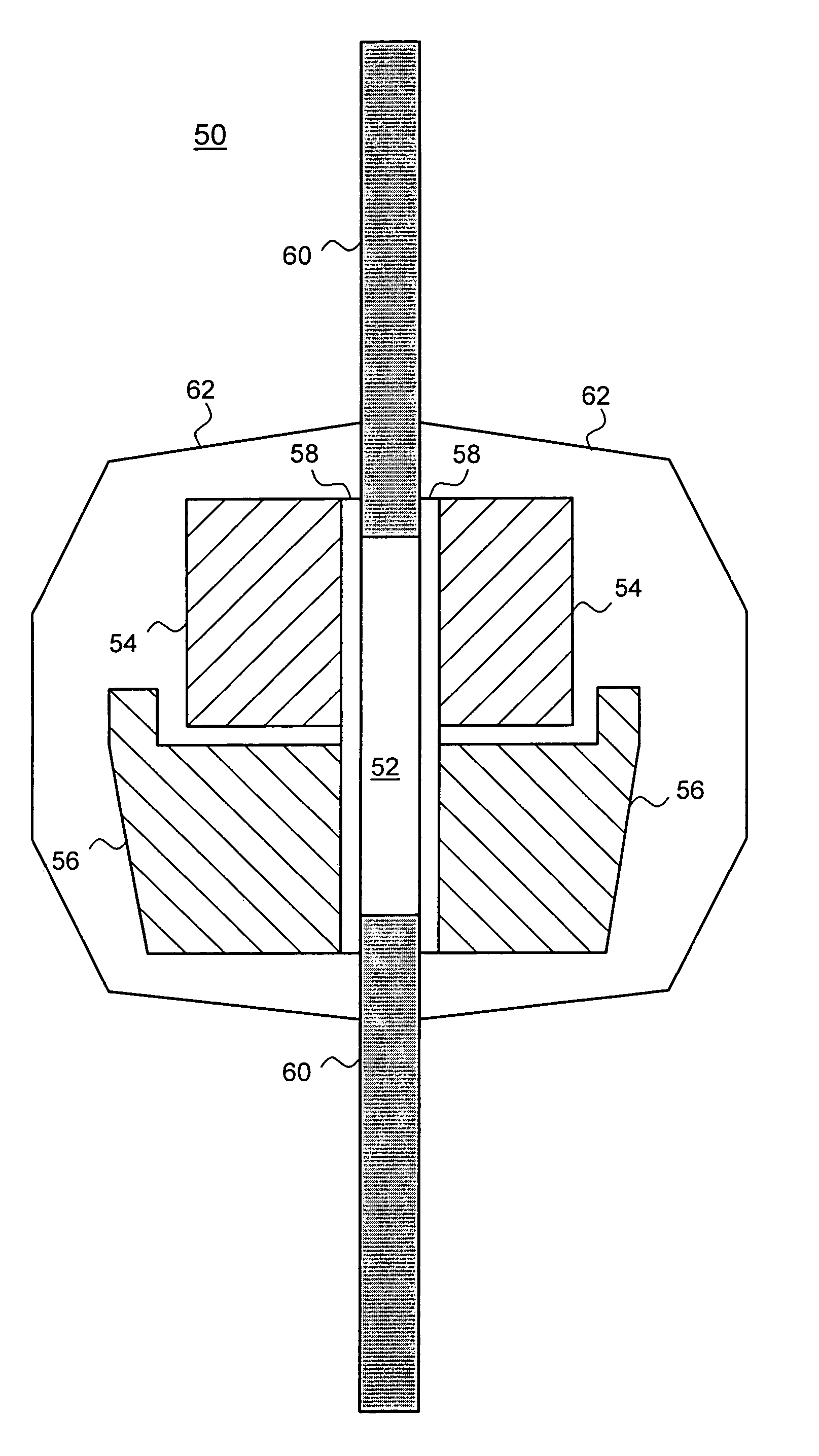
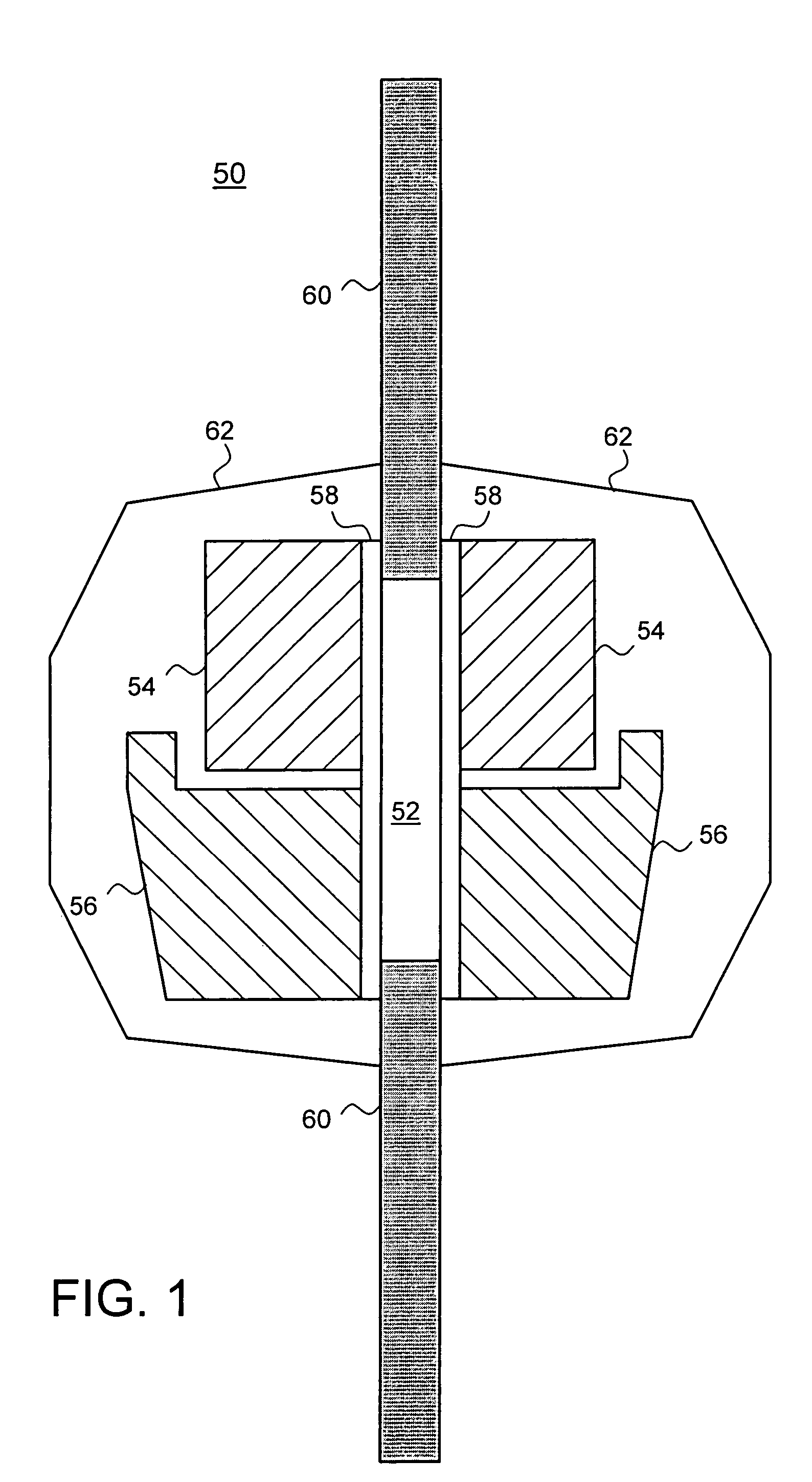
[0019]The present invention provides a dual gate transistor and a method for forming the same that results in improved device performance and density. The present invention uses a double gate design to implement a dual gate transistor. A double gate is a gate which is formed on both sides of the transistor body. The present invention thus provides a transistor with two double gates in series that provide improved current control over traditional dual gate designs. The preferred embodiment of the present invention uses a fin type body with dual double-gates. In a fin type structure, the double gates are formed on each side of a thin fin shaped body, with the body being disposed horizontally between the gates.

[0020]In another aspect of the invention, the dual double gates are provided with offset gaps between the double gates. The offset of the gaps allows the size of the gaps to be increased, reducing gate to gate capacitance, while still providing exceptional current control.

[0021]T...


PUM


Abstract

The present invention provides a dual gate transistor and a method for forming the same that results in improved device performance and density. The present invention uses a double gate design to implement a dual gate transistor. A double gate is a gate which is formed on both sides of the transistor body. The present invention thus provides a transistor with two double gates in series that provide improved current control over traditional dual gate designs. The preferred embodiment of the present invention uses a fin type body with dual double-gates. In a fin type structure, the double gates are formed on each side of a thin fin shaped body, with the body being disposed horizontally between the gates.

Description

[0001]This application is a divisional of Ser. No. 10 / 063,323; filed on Apr. 11, 2002, now U.S Pat. No. 6,750,487.BACKGROUND OF THE INVENTION[0002]1. Technical Field[0003]The present invention relates generally to the field of semiconductor manufacturing and, more specifically, to a method for forming double gated field effect transistors.[0004]2. Background Art[0005]The need to remain cost and performance competitive in the production of semiconductor devices has caused continually increasing device density in integrated circuits. To facilitate the increase in device density, new technologies are constantly needed to allow the feature size of these semiconductor devices to be reduced.[0006]The push for ever increasing device densities is particularly strong in CMOS technologies, such as the in the design and fabrication of field effect transistors (FETs). FETs are used in almost all types of integrated circuit design (i.e., microprocessors, memory, etc.) Unfortunately, increased de...

Claims


Application Information

Patent Timeline
IPC IPC(8): H01L21/337H01L21/336H01L29/423H01L29/786
CPCH01L29/42384H01L29/785H01L29/66795H01L29/7856
Inventor FRIED, DAVID M.NOWAK, EDWARD J.
Owner GLOBALFOUNDRIES US INC
Why Eureka
Try Eureka