Substrate processing device and processing method

a processing device and substrate technology, applied in the direction of microstructural devices, manufacturing tools, coatings, etc., can solve the problems of mechanical structure damage, mechanical structure, switching function damage, etc., and achieve the effect of high reliability

Inactive Publication Date: 2006-09-05
TOKYO ELECTRON LTD
View PDF21 Cites 55 Cited by
  • Summary
  • Abstract
  • Description
  • Claims
  • Application Information

AI Technical Summary

Benefits of technology

[0012]In view of the above situations, an object of the present invention is to provide a substrate processing device and processing method capable of processing a substrate having a fine structure on the surface thereof with a high reliability.
[0013]Another object of the present invention is to provide a substrate processing device and processing method capable of processing a substrate having a fine structure on the surface thereof, while reducing damages on the fine structure and its function.

Problems solved by technology

However, a mechanical structure is exposed on the surface of the MEMS element substrate, and this causes the following problems if the above-described conventional processing method is used.
First, in case of a cutting process using a dicing saw, minute cutting dust produced from cutting stick to the mechanical structure, causing a fear that the function of the mechanical structure might be damaged.
For example, if minute cutting dust enter a space between a cantilever and the surface of a substrate, the switching function of a switching element might be harmed.
Because of this, the mechanical structure, which is exposed on the surface of the substrate might be damaged by the flow of the water.
Third, the function of the mechanical structure might be damaged by the surface tension of the water when the water evaporates.
For example, if a cantilever is stuck on the surface of a substrate, the switching function of a switching element might be damaged.
As described above, in a case where a substrate on which an MEMS element is formed is processed by utilizing the above-described conventional method, there is a danger that the mechanical structure exposed on the surface of the substrate and its function might be damaged.
This might damage the reliability of substrate processing, and cause a decrease in the yield.

Method used


Image

  • Substrate processing device and processing method
  • Substrate processing device and processing method
  • Substrate processing device and processing method

Examples


Embodiment Construction

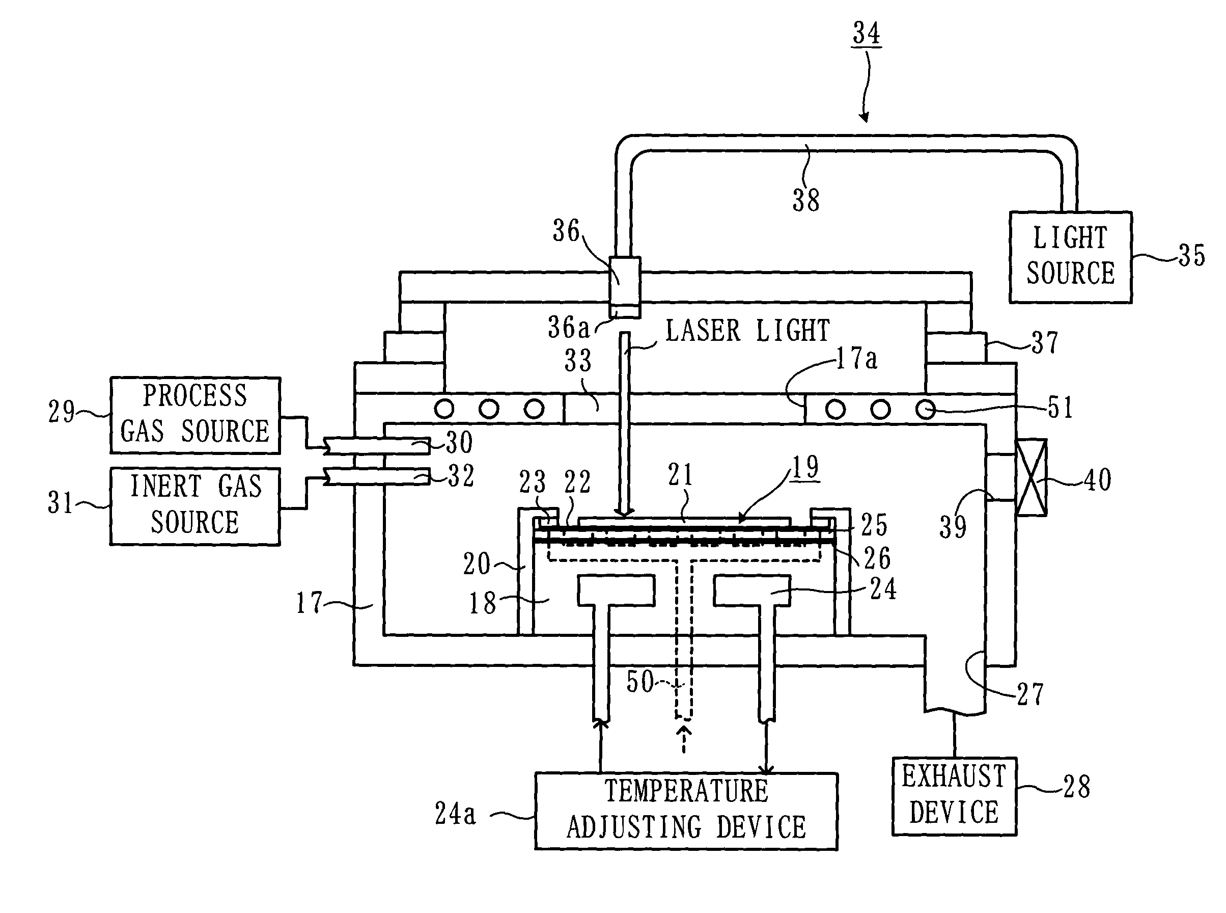
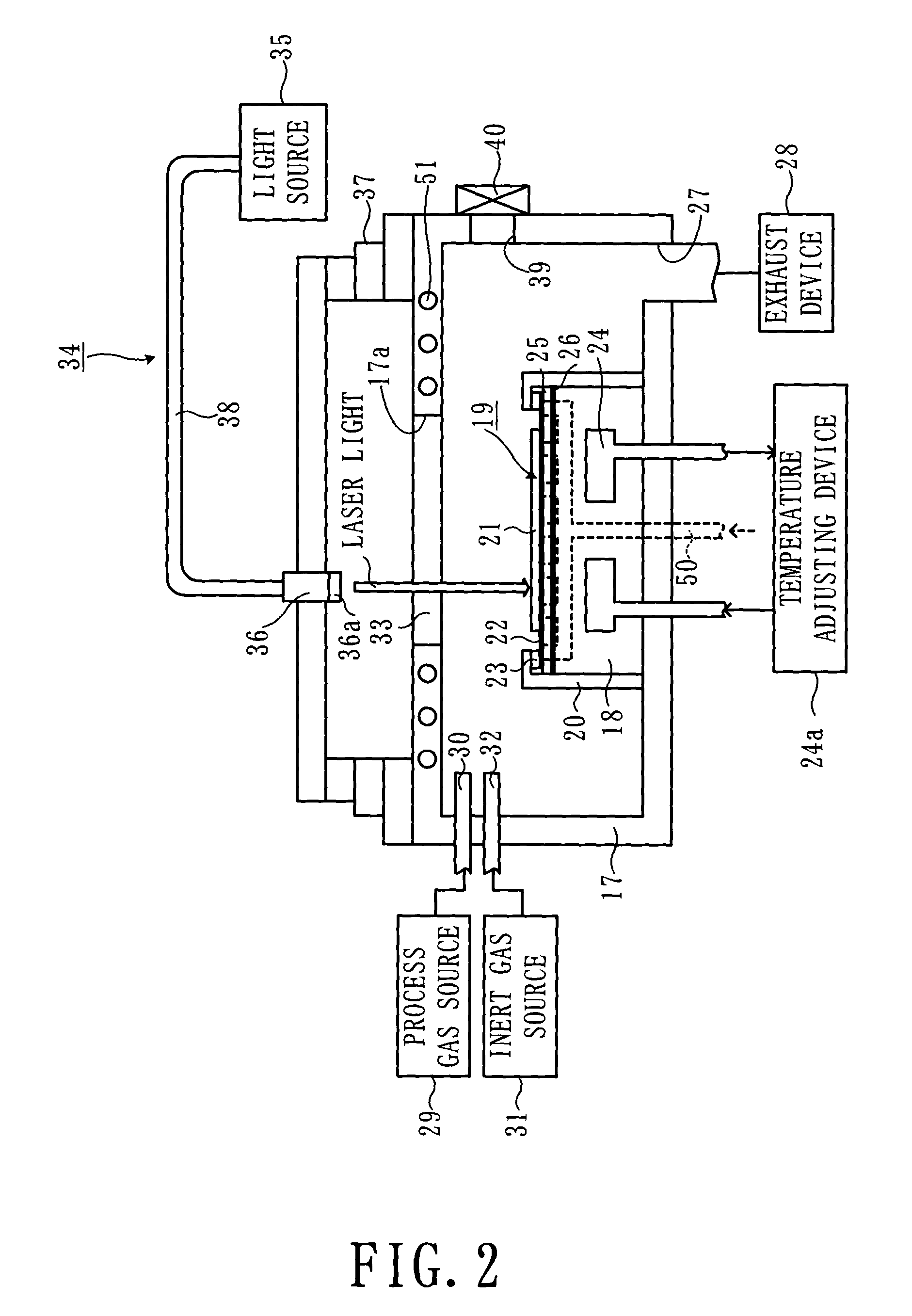
[0058]A substrate processing device and processing method according to an embodiment of the present invention will now be explained with reference to the drawings. In the present embodiment, a case where the present invention is applied to a dicing device and a dicing method for applying a dividing process to a semiconductor substrate, will be explained as an example.

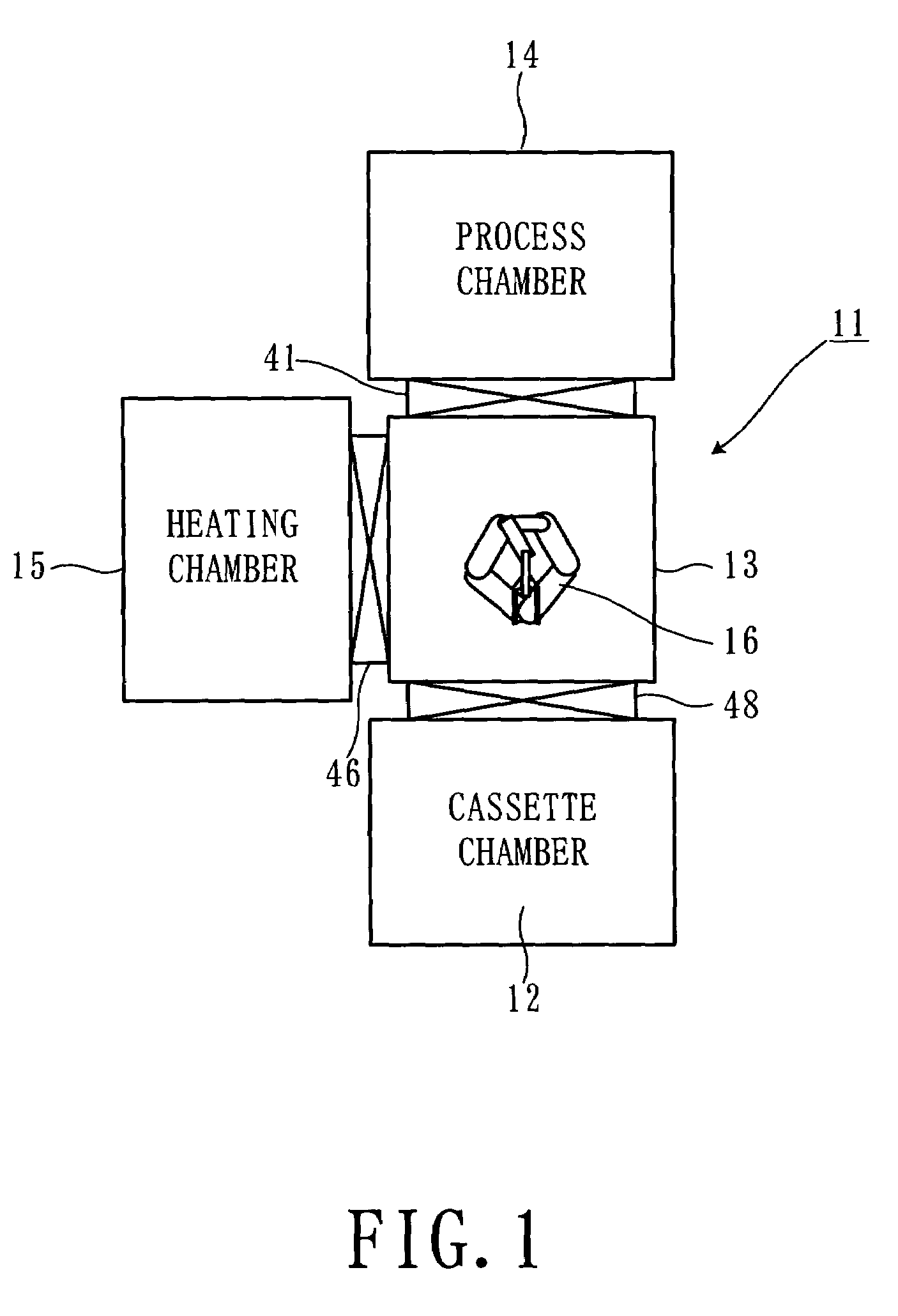
[0059]The structure of a processing device 11 according to the present embodiment is shown in FIG. 1.

[0060]As shown in FIG. 1, the processing device 11 comprises a cassette chamber 12, a transportation chamber 13, a process chamber 14, and a heating chamber 15.

[0061]The cassette chamber 12 functions as a port for transporting a cassette into and out from the processing device 11. The cassette chamber 12 has a cassette stand or the like, and is structured so that a predetermined number of cassettes can be set thereinside. A semiconductor substrate (hereinafter, referred to as process target) which is adhered to a frame b...


PUM

PropertyMeasurementUnit
temperatureaaaaaaaaaa
thicknessaaaaaaaaaa
anglesaaaaaaaaaa

Abstract

In a state where a process gas including SF.sub. 6 and O.sub. 2 is supplied in a chamber, a laser light irradiator provided outside the chamber irradiates a laser light onto a substrate. At the portion of the substrate onto which the laser light is irradiated, the material that makes up the substrate is excited and converted into a gaseous substance by reacting with the process gas. The temperature of the substrate placed on a stage is kept at a predetermined temperature since a temperature adjuster supplies a chiller to a coolant flow passage provided inside the stage.

Description

BACKGROUND OF THE INVENTION[0001]1. Field of the Invention[0002]The present invention relates to a processing device and a processing method for a substrate such as a semiconductor substrate.[0003]2. Description of the Related Art[0004]A method using a dicing saw which is rotated at a high speed is widely used as a method of applying some process, for example, dividing to a substrate such as a semiconductor substrate. According to this method, a substrate in a state of being adhered on an adhesive sheet is cut by a dicing saw made of a diamond blade, etc.[0005]There is a kind of semiconductor element called MEMS (Micro Electro Mechanical System) element. The MEMS element comprises a mechanical structure which is formed on a surface of a semiconductor substrate in which circuit elements are formed. The MEMS element is used for an electronic component and a mechanical component necessary for many types of electronic systems and electronic optical systems. For example, an optical switc...

Claims


Application Information

Patent Timeline
Patent Type & Authority Patents(United States)
IPC IPC(8): H01L21/302H01L21/301B28D5/00B81C1/00H01L21/00
CPCH01L21/67115H01L21/67092
Inventor YUASA, MITSUHIRO
Owner TOKYO ELECTRON LTD
Why Eureka
Try Eureka