Photodiode that reduces the effects of surface recombination sites

a photodiode and surface recombination technology, applied in the field of photodiodes, can solve the problems of limiting the photodiode to only collecting a single color, increasing the magnitude of the integrated voltage, and reducing the total number of collected electrons

Active Publication Date: 2006-09-12
NAT SEMICON CORP
View PDF17 Cites 14 Cited by
  • Summary
  • Abstract
  • Description
  • Claims
  • Application Information

AI Technical Summary

Problems solved by technology

This is due to the solid solubility and the tendency of indium to precipitate out.
Thus, although a black and white photodiode is capable of capturing a wider range of the visible light spectrum, the color filter limits the photodiode to collecting only a single color.
The lost electrons reduce the total number of collected electrons which erroneously increases the magnitude of the integrated voltage.

Method used


Image

  • Photodiode that reduces the effects of surface recombination sites
  • Photodiode that reduces the effects of surface recombination sites
  • Photodiode that reduces the effects of surface recombination sites

Examples


Embodiment Construction

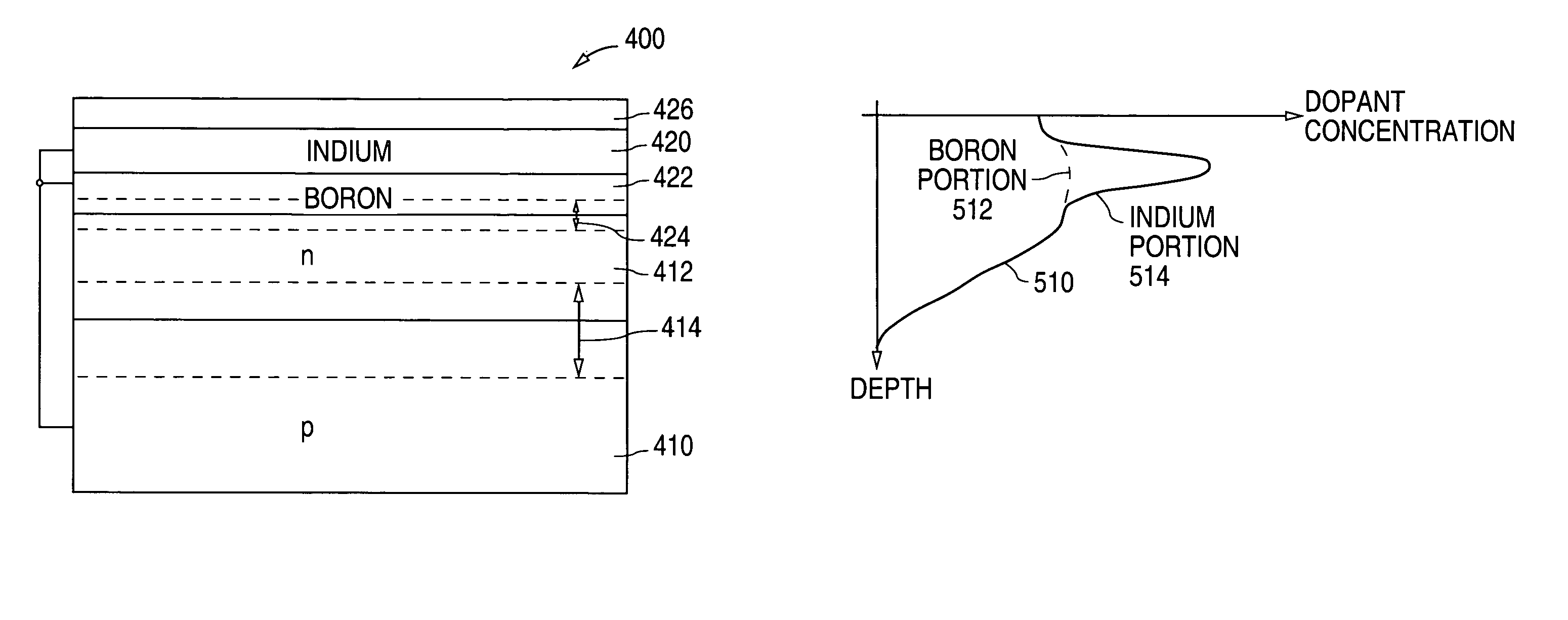
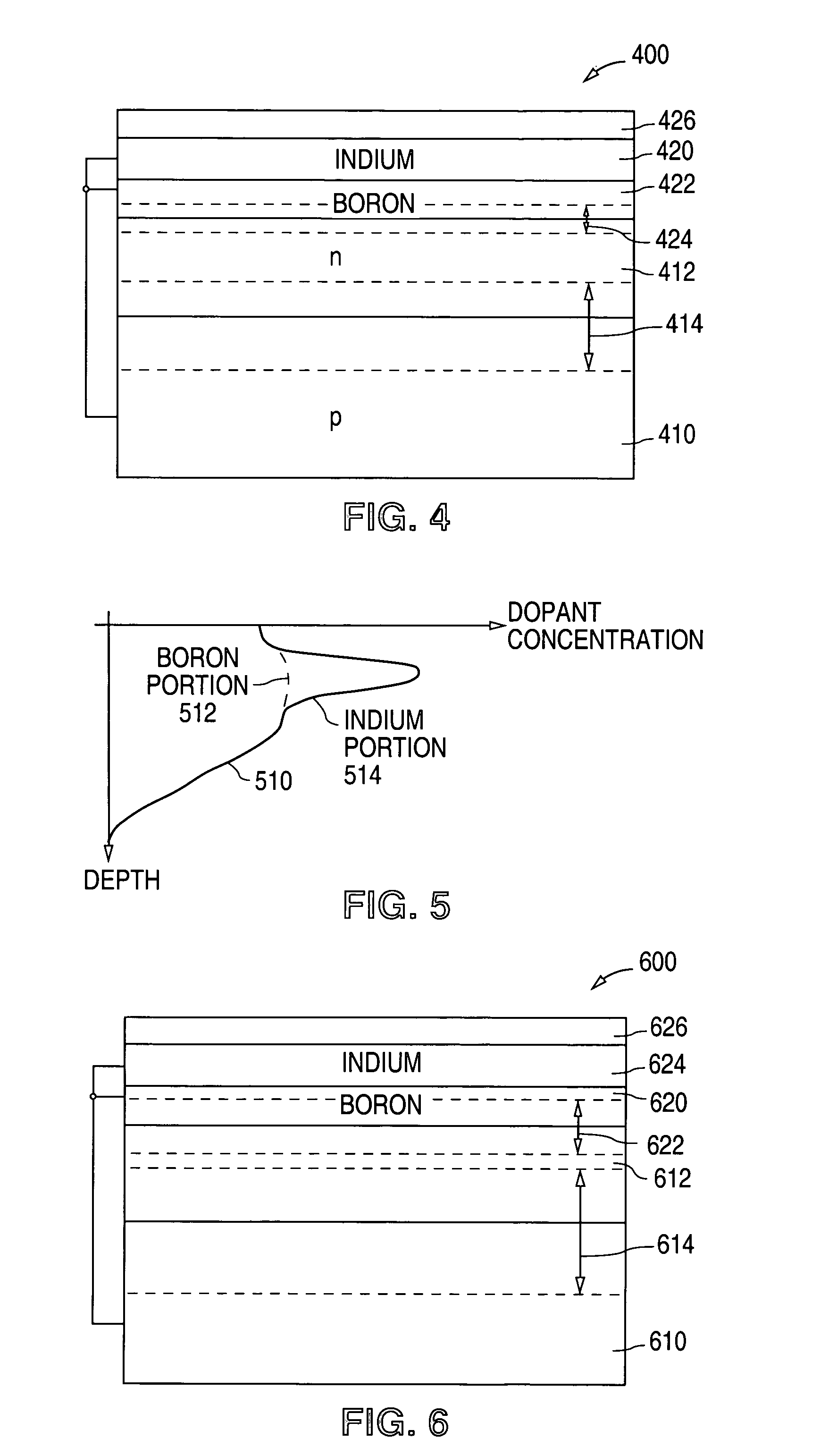
[0028]FIG. 4 shows a cross-sectional diagram that illustrates an example of a blue photodiode 400 in accordance with the present invention. As described in greater detail below, blue photodiode 400 utilizes a p-type surface region to form a barrier that repels photogenerated electrons from the surface electron-hole recombination sites.

[0029]As shown in FIG. 4, blue photodiode 400 includes a first p-type (boron) region 410, such as a substrate, a second n-type region 412, such as an epitaxial layer or well, that overlies and contacts p-type region 410, and a depletion region 414 that is formed across the pn junction between p-type region 410 and n-type region 412.

[0030]In the present example, n-type region 412 has a moderate dopant concentration, such as 5×10¹⁷ to 1×10¹⁸ atoms / cm3, that is approximately equal to the dopant concentration of a lightly-doped-drain (LDD) region. Alternately, n-type region 412 can be formed to have a heavier (n+), e.g., 1×10¹⁹ to 1×10²⁰ atoms / cm3, (or lig...


PUM


Abstract

The loss of photogenerated electrons to surface electron-hole recombination sites is minimized by utilizing a first p-type surface region to form a depletion region that functions as a first barrier that repels photogenerated electrons from the surface recombination sites, and a second p-type surface region that provides a substantial change in the dopant concentration.

Description

BACKGROUND OF THE INVENTION[0001]1. Field of the Invention[0002]The present invention relates to photodiodes and, more particularly, to a photodiode that reduces the effects of the surface electron-hole recombination sites.[0003]2. Description of the Related Art[0004]A p-type material is a semiconductor material, such as single-crystal silicon, that includes impurity “acceptor” atoms (atoms that are missing one electron in their outer shell). All of the column IIIA elements (group 13) (Boron, Aluminum, Gallium, Indium, and Thalium) have one missing electron in the outer shell and are acceptor atoms.[0005]FIG. 1 shows a graph that illustrates the dopant profiles of the column IIIA elements in silicon when implanted at the same dose at the same energy for the same amount of time. As shown in FIG. 1, as the size of the atom increases, the depth of the implant decreases. As a result, the element boron, which is the smallest atom, has the deepest implant.[0006]FIG. 2 shows a graph that i...

Claims


Application Information

Patent Timeline
Patent Type & Authority Patents(United States)
IPC IPC(8): H01L31/113H01L21/00H01L21/76H01L29/76
CPCH01L31/0352H01L31/1868H01L31/103H01L31/02162Y02E10/50
Inventor HOPPER, PETER J.MIAN, MICHAELDRURY, ROBERT
Owner NAT SEMICON CORP
Why Eureka
Try Eureka