
Waveguide device

a waveguide and device technology, applied in the field of waveguide devices, can solve the problems of unwanted coupling loss in the optical connection, unwanted radiation loss at the outside of the waveguide, and the core dimension of the waveguide requires additional regions, so as to achieve the effect of less optical coupling loss and small siz

Inactive Publication Date: 2006-09-12
NEC CORP
View PDF18 Cites 0 Cited by
  • Summary
  • Abstract
  • Description
  • Claims
  • Application Information

AI Technical Summary

Benefits of technology

[0012]An object of the present invention is to provide waveguide chips and waveguide devices, which have one or more bent waveguides, and which are small in size and are subject to less optical coupling loss at the optical connection to the optical fibers.

Problems solved by technology

However, the small bending radius of curvature causes unwanted radiation loss at the outside of the waveguide in the bend.
This causes unwanted coupling loss in the optical connection.
However, gradually changing the core dimension of the waveguide requires additional regions in the waveguide devices.
This causes a new problem that the waveguide chip tends to be increased in size.

Method used


Image

  • Waveguide device
  • Waveguide device
  • Waveguide device

Examples


Embodiment Construction

[0043]Preferred embodiments of the present invention will now be described with reference to the drawings.

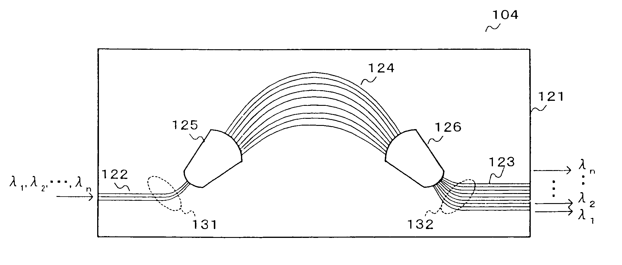
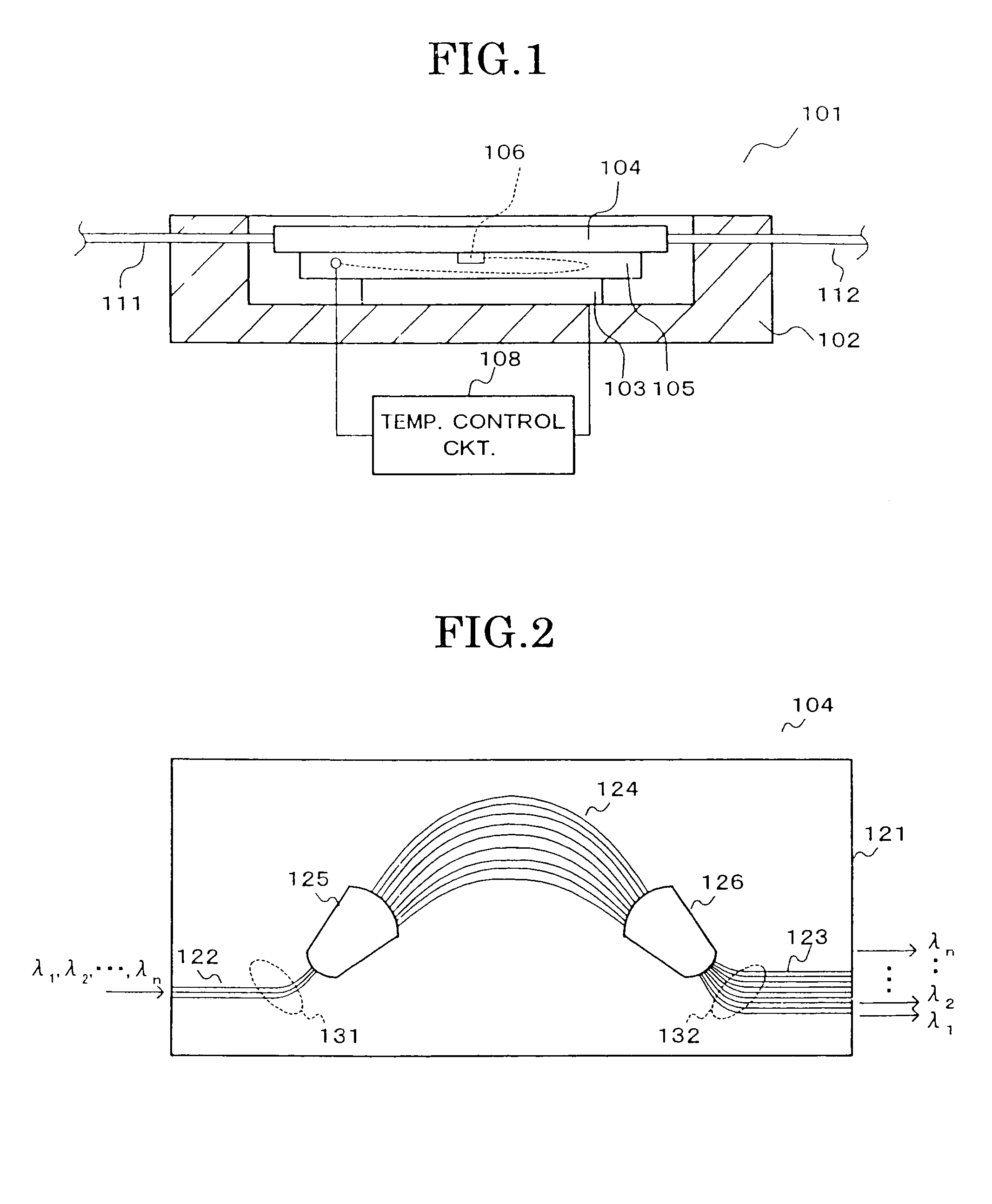
[0044]FIG. 1 shows essential parts of an arrayed waveguide grating module in a waveguide device as an embodiment of the present invention. The arrayed waveguide grating module comprises a boxing case 102, a temperature control element 103 constituted by a Peltier element mounted on the bottom of the case 102 for heating or cooling the module, an arrayed waveguide grating 104 and a metal plate 105 intervening between the components 103 and 104. The metal plate 105 is greater in size than the contact size of the temperature control element 103 for increasing the temperature control region of the temperature control element 103. A temperature sensor 106 is embedded in the metal plate 105. The temperature sensor 106 provides a temperature detection output, which is inputted to a temperature control circuit 108 for temperature control by the temperature control element 103.

[0045]Opti...


PUM


Abstract

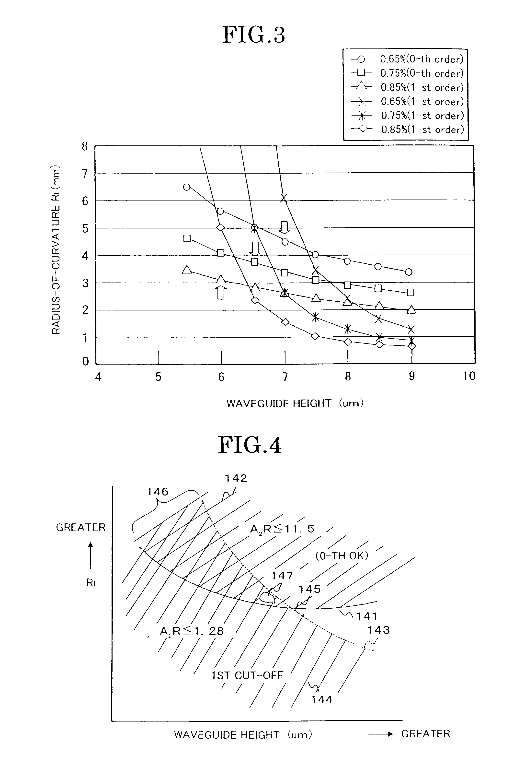
Bent waveguide parts 131 and 132 on a substrate 121 of an arrayed waveguide chip 104 have a core dimension allowing multi-mode operation, but they are adapted to constitute higher order mode filters with adequate combination of the relation of the height and width of waveguides and the minimum radius of curvature. Thus, with the multi-mode as preamble it is possible to cut off higher order mode light propagation by setting a small minimum radius of curvature, thus realizing single-mode light propagation and reducing the optical coupling loss through optical fibers 111 and 112. Thus, it is possible to realize a waveguide chip and a waveguide device with the minimum radius of curvature of bent waveguides and less optical coupling loss in connection parts to optical fibers.

Description

BACKGROUND OF THE INVENTION[0001]This application claims benefit of Japanese Patent Application No. 2002-046324 filed on Feb. 22, 2002, the contents of which are incorporated by the reference.[0002]The present invention relates to waveguide devices, in which optical fibers are optically connected to waveguide elements such as AWG (arrayed waveguide grating) and Mach-Zehnder interferometer and, more particularly, to waveguide devices adapted to reduce or eliminate optical coupling loss in such optical connection parts.[0003]Recent rapid growth in the traffic of the Internet or telecommunication network systems demands high transmission speed and large capacity in the trunk transmission systems, called backbones. DWDM (Dense Wavelength Division Multiplexing) systems, in which multiple optical signals in different wavelengths are multiplexed, are useful to build large capacity transmission systems. The DWDM systems use waveguide devices such as AWGs for processing optical signals for m...

Claims


Application Information

Patent Timeline
IPC IPC(8): G02B6/26G02B6/34G02B6/42G02B6/122G02B6/12G02B6/125G02B6/126
CPCG02B6/12007G02B6/125G02B6/12026
Inventor HANADA, TADAHIKO
Owner NEC CORP
Learn More