Semiconductor memory device having a circuit for removing noise from a power line of the memory device using a plurality of decoupling capactors

a technology of decoupling capactors and memory devices, which is applied in the direction of power supply for data processing, liquid/fluent solid measurement, instruments, etc., can solve the problems of increasing the size of the chip, affecting the amount of charges stored in the cell capacitors, and dram malfunction

Inactive Publication Date: 2006-09-12
SAMSUNG ELECTRONICS CO LTD
View PDF10 Cites 15 Cited by
  • Summary
  • Abstract
  • Description
  • Claims
  • Application Information

AI Technical Summary

Problems solved by technology

If external influences cause the amount of charges stored in the cell capacitor to vary, the data of the memory cell can be misread, resulting in a DRAM malfunction.
Once source of malfunctions is the introduction of noise into the internal power line of the DRAM to such an extent that a resultant fluctuation in the power supply voltage level adversely effects the amount of charges stored in the cell capacitors.
However, since each MOS decoupling capacitor has a low electrostatic capacity, many capacitors are needed to obtain an overall electrostatic capacity which is sufficient to remove power noise.
Hence, the decoupling capacitors constitute overhead which increases the size of the chip.
In addition, current leakage through an MOS decoupling capacitor can occur if the capacitor contains a defective insulating oxide film, resulting in DRAM malfunctions.
Conventional power noise removing circuits cannot completely isolate such defective decoupling capacitors from the power lines.

Method used


Image

  • Semiconductor memory device having a circuit for removing noise from a power line of the memory device using a plurality of decoupling capactors
  • Semiconductor memory device having a circuit for removing noise from a power line of the memory device using a plurality of decoupling capactors
  • Semiconductor memory device having a circuit for removing noise from a power line of the memory device using a plurality of decoupling capactors

Examples


Embodiment Construction

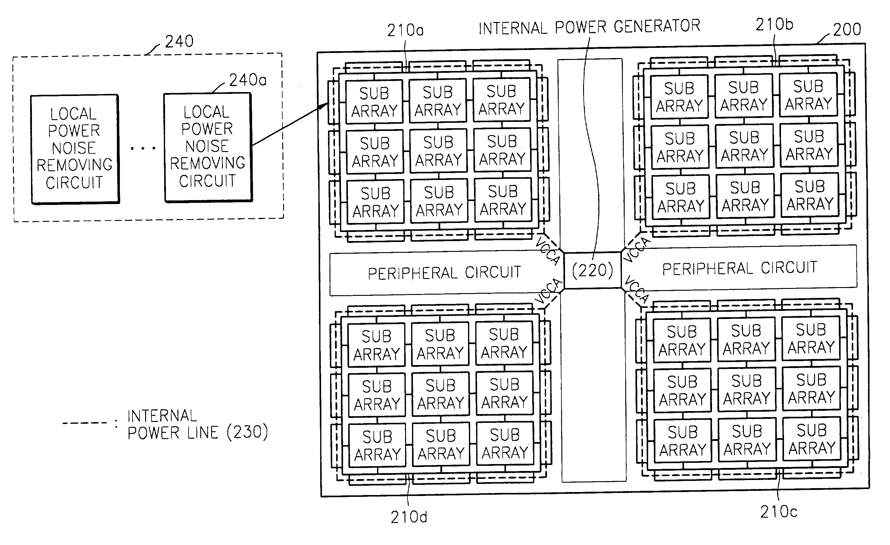
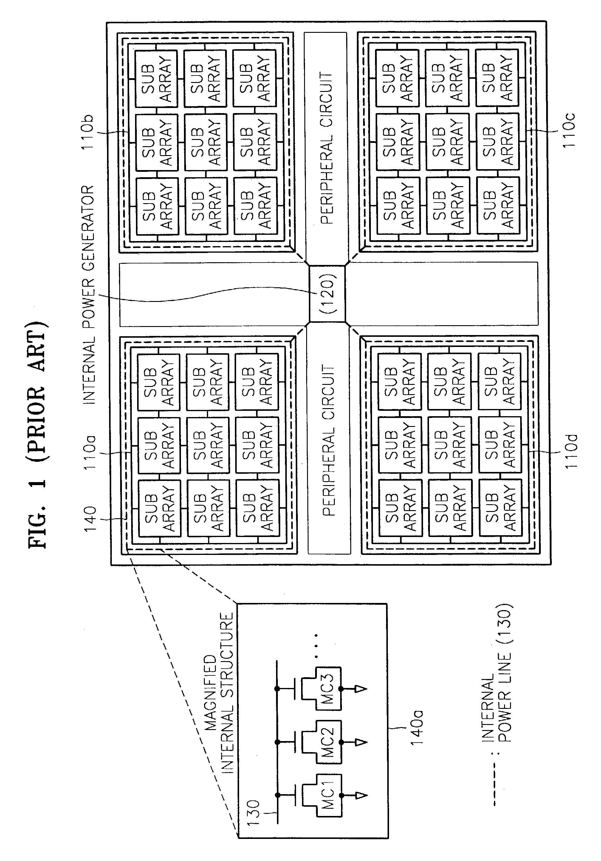
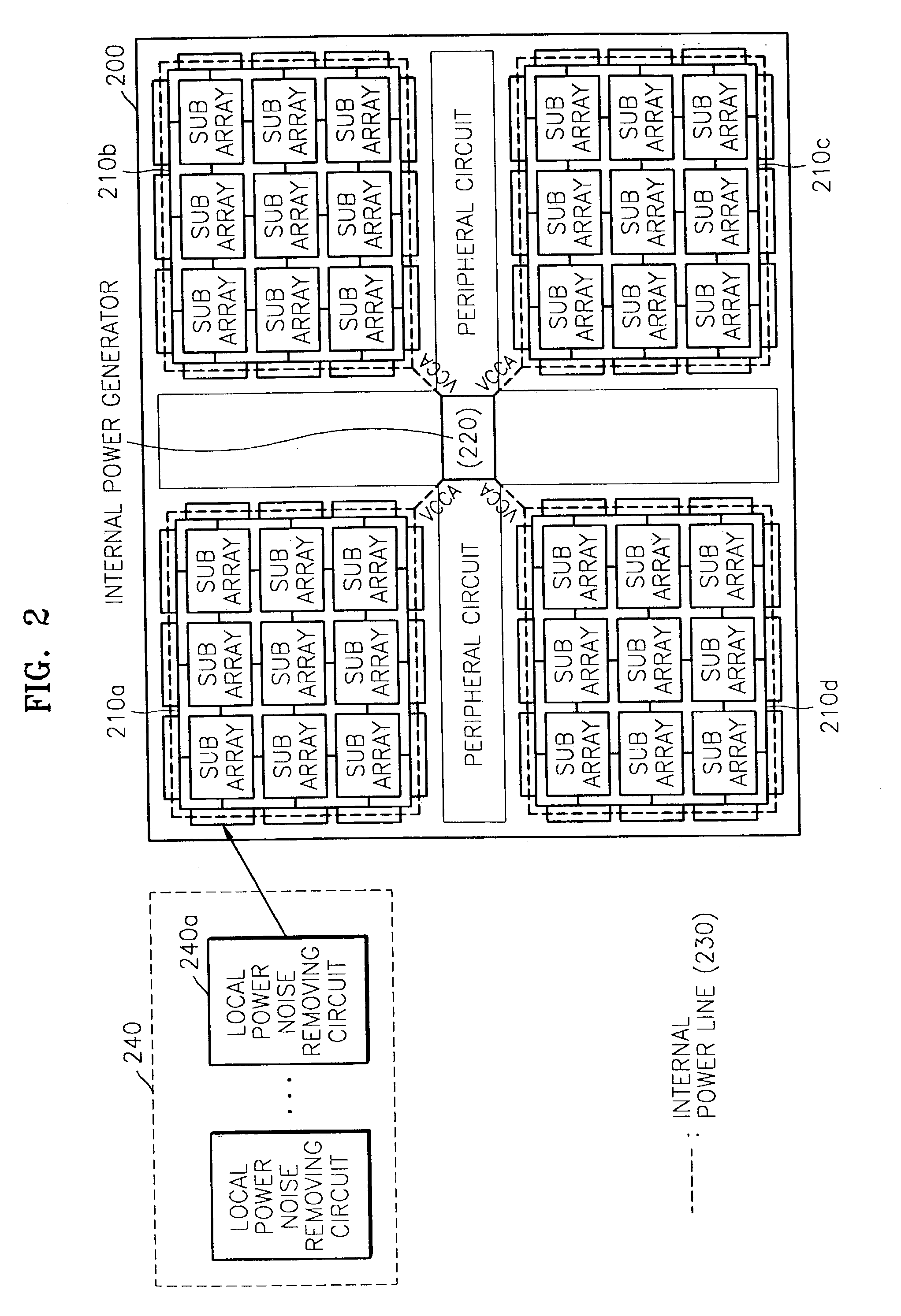
[0027]As described above, since the MOS transistor type decoupling capacitor has a small electrostatic capacity, the conventional technique is to couple a large number of such capacitors to the internal power line in an effort to reduce noise induced fluctuations. This adversely increases the size of the chip. To overcome this problem, according to one aspect of the present invention, decoupling capacitors are constituted by cell capacitors of the DRAM cell. DRAM cell capacitors occupy a significantly smaller area in the chip and exhibit a higher capacitance than MOS transistor type capacitors.

[0028]According to another aspect of the present invention, the decoupling capacitors are partitioned into at least two groups, and individual decoupling capacitor groups are tested to determine if they are defective, for example, to determine if there current leakage caused by a defective dielectric layer. Any defective decoupling capacitor group is then isolated from the others.

[0029]The pre...


PUM


Abstract

The power noise removing circuit includes a decoupling capacitor group, a repair circuit unit, a monitoring pad, and a testing unit. The decoupling capacitor group includes a plurality of decoupling capacitors that store noise flowing into an internal power line. The decoupling capacitors are DRAM cell type capacitors. The repair circuit unit controls a connection of each of the decoupling capacitors in the decoupling capacitor group to an external input power line. The monitoring pad measures the amount of current leaking from the decoupling capacitor group. The testing unit controls a connection of the decoupling capacitor group to the monitoring pad. If the decoupling capacitor group is tested as being defective, the defective decoupling capacitor group is made inoperative by disconnection from the external input power line.

Description

BACKGROUND OF THE INVENTION[0001]1. Field of the Invention[0002]The present invention relates to semiconductor devices, and more particularly, to a circuit for removing noise from the internal power line of a semiconductor device in order to minimize fluctuations in an internal voltage of the semiconductor device.[0003]2. Description of the Related Art[0004]Together with advancements in semiconductor memory design and processing techniques, semiconductor integrated circuits capable of operating at low operating voltages have been developed. For example, in dynamic random access memories (DRAMs) contained in portable electronic or / and communication equipment, the operating voltage has recently been lowered to 1.0V or less.[0005]Each memory cell of a DRAM includes an access transistor which performs a switching function, and a capacitor (hereinafter, referred to as a cell capacitor) connected to the access transistor. Reading and writing of the DRAM is carried by selectively storing c...

Claims


Application Information

Patent Timeline
Patent Type & Authority Patents(United States)
IPC IPC(8): G06F1/26G11C29/00G11C7/02G11C11/4074G11C29/02
CPCG11C11/4074G11C29/12005G11C29/02G11C11/401G11C2029/5006G11C29/00
Inventor LEE, HI-CHOONKIM, KYUNG-HO
Owner SAMSUNG ELECTRONICS CO LTD
Why Eureka
Try Eureka