Integrated circuit component, protected against random logic events, and associated method of manufacture

a technology of integrated circuits and components, applied in pulse generators, pulse techniques, instruments, etc., can solve problems such as voltage or current spikes at a point of the circuit, random logic events, and circuits becoming increasingly sensitive to external environmen

Inactive Publication Date: 2006-09-19
STMICROELECTRONICS SRL
View PDF11 Cites 10 Cited by
  • Summary
  • Abstract
  • Description
  • Claims
  • Application Information

AI Technical Summary

Benefits of technology

[0029]One aspect of the invention proposes a novel solution, without the drawbacks of the solution proposed by D1, for the protection of an integrated circuit component against random logic events by increasing its critical charge.
[0035]The critical charge of the component in this case is fixed as a function of the capacitance of the capacitors, the potentials applied to the first node and the second node, and the fixed potential at the control terminal. It is then possible to fix the potential at the common point of the two capacitors from the exterior. This makes it possible to modulate the critical charge of the component as a function of the medium in which it is used (namely as a function of its use in terrestrial applications, space applications, etc.).
[0044]Preferably, the second capacitor is made so as to be substantially identical to the first capacitor. Thus a perfectly symmetrical component is obtained, and the manufacturing process is simplified.

Problems solved by technology

This means, however, that the circuits are becoming increasingly sensitive to their external environment and especially to random logic events caused by an additional supply of energy from outside the circuit.
This is no longer the case for integrated circuits whose components have dimensions smaller than 0.5 micrometers because the circuits become increasingly sensitive as their dimensions decrease.
This generally results in a voltage or current spike at a point of the circuit (impact point in the case of an SEU, or a coupling point in the case of a glitch).
However, it may give rise to a random logic event if the added charge is greater than the critical charge of the circuit.
The critical charge of a circuit is especially small as the technology used to make it is small.

Method used


Image

  • Integrated circuit component, protected against random logic events, and associated method of manufacture
  • Integrated circuit component, protected against random logic events, and associated method of manufacture
  • Integrated circuit component, protected against random logic events, and associated method of manufacture

Examples


Embodiment Construction

[0058]The following discussion is presented to enable a person skilled in the art to make and use the invention. Various modifications to the embodiments will be readily apparent to those skilled in the art, and the generic principles herein may be applied to other embodiments and applications without departing from the spirit and scope of the present invention as defined by the appended claims. Thus, the present invention is not intended to be limited to the embodiments shown, but is to be accorded the widest scope consistent with the principles and features disclosed herein.

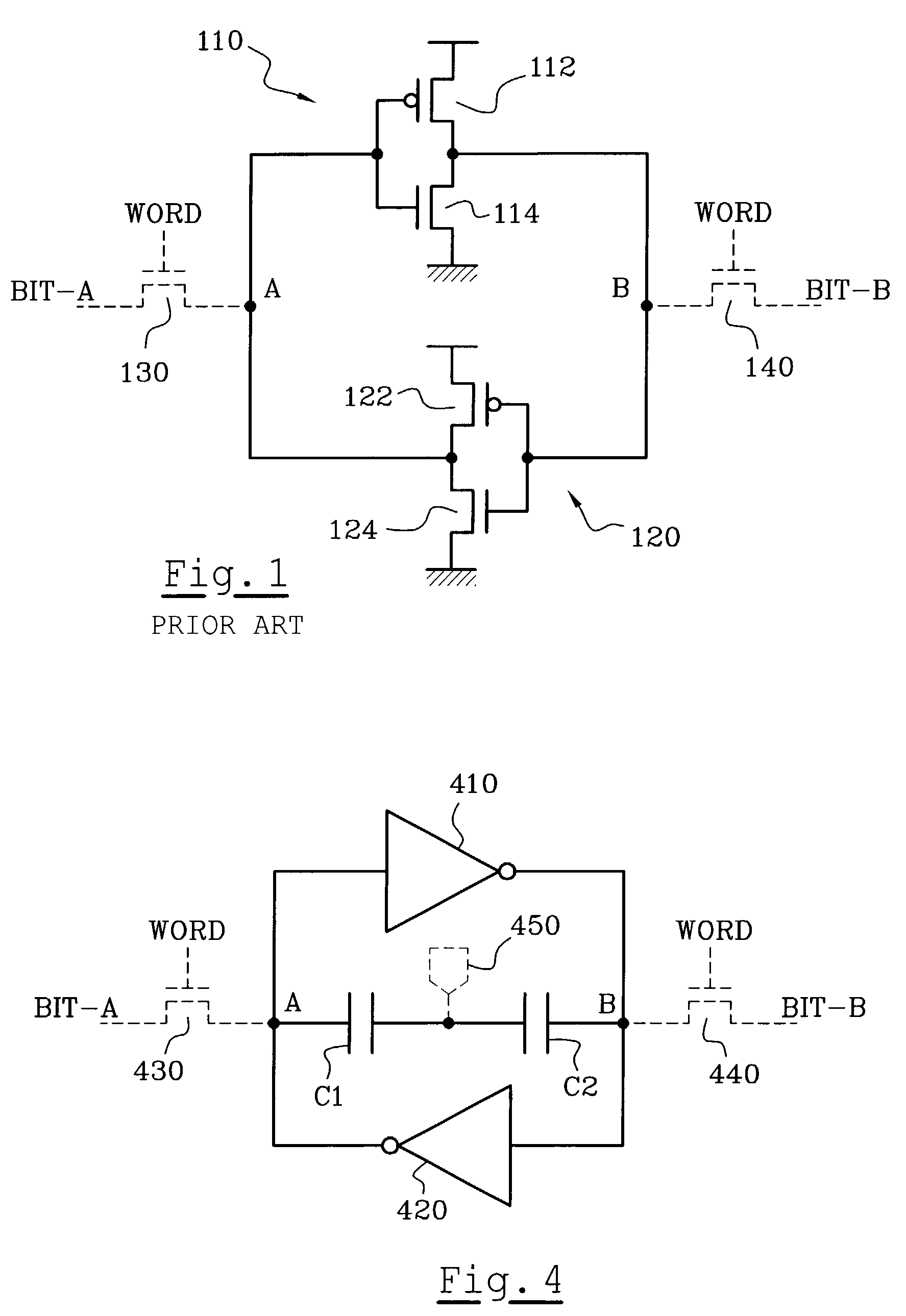
[0059]A first exemplary implementation of an embodiment of the invention (not shown) relates to the making of a combinatorial logic circuit or dynamic logic circuit protected against random events. As compared with an existing equivalent circuit, this circuit has two series-connected capacitors added between two sensitive nodes of the circuit, or else between a sensitive node and a power supply input terminal, ...


PUM


Abstract

A component of an integrated circuit comprises a first capacitor and a second capacitor series-connected between a first node and a second node of the component. This has application to logic circuits and bistable circuits, for example, SRAM type memories, flip-flop trigger circuits, etc.

Description

CROSS-REFERENCE TO RELATED APPLICATIONS[0001]The present application claims priority from French patent application No. 01 16072, filed Dec. 13, 2001, which is incorporated by reference.BACKGROUND OF THE INVENTION[0002]1. Field of the Invention[0003]The invention relates generally to a component of an integrated circuit protected against random logic events and an associated method of manufacture. The component may be a storage cell, for example, a multipoint memory cell, a latch, RS or flip-flop type trigger circuit or an SRAM cell. The component may also be logic circuit, for example, a combinatorial logic circuit or a dynamic logic circuit.[0004]Embodiments of the invention is particularly useful for the making of electronic devices whose components are designed with dimensions smaller than 0.25 μm.[0005]2. Description of the Prior Art[0006]The constant and gradual miniaturization of electronic circuits is giving rise to increasingly efficient and ever smaller circuits. This mean...

Claims


Application Information

Patent Timeline
Patent Type & Authority Patents(United States)
IPC IPC(8): H01L21/70G11C11/412H01L27/11H03K3/037
CPCG11C11/4125H03K3/0375H01L27/1104H10B10/12
Inventor JACQUET, FRANCOISROCHE, PHILLIPESCHOELLKOPF, JEANNE-PIERRE
Owner STMICROELECTRONICS SRL
Why Eureka
Try Eureka