Sealing structure with barrier membrane for electronic element, display device, electronic apparatus, and fabrication method for electronic element

a technology of electronic elements and sealing structures, applied in discharge tubes/lamp details, discharge tubes luminescnet screens, other domestic articles, etc., can solve the problems of reducing the overall size affecting the exterior design affecting the display effect of the display device, so as to achieve adequate barrier properties and prevent penetration performance of edges

Inactive Publication Date: 2006-09-19
SEIKO EPSON CORP
View PDF32 Cites 27 Cited by
  • Summary
  • Abstract
  • Description
  • Claims
  • Application Information

AI Technical Summary

Benefits of technology

[0066]According to the above method for fabricating a display device, because the edges of the multi-layered sealing membrane can be formed in such a manner that the edges of the flattening resin layers and the barrier layers, which are alternatel...

Problems solved by technology

Moreover, because adhesive is used to adhere the “sealing can” to the substrate, a region for applying the adhesive must be occupied along the periphery of the substrate, and as a result, the size of the region for display, in which the display elements are arranged, is reduced with respect to the overall size of the display device, whereby a problem is encountered in that the exterior design of the display device is constrained when the display device is employed as a display portion of an electronic apparatus such as a portable telephone or the like.
In addition, an allowable space must be occupied between the region for applying the adhesive and the region for display because the adhesive may spread out, which leads to another problem in conventional display devices in that the size of a so-called frame region, i.e., a region formed by the allowable space and the region for applying the adhesive, cannot be reduced.
Furthermore, if the size of the region for applying the adhesive is reduced in order to enlarge ...

Method used


Image

  • Sealing structure with barrier membrane for electronic element, display device, electronic apparatus, and fabrication method for electronic element
  • Sealing structure with barrier membrane for electronic element, display device, electronic apparatus, and fabrication method for electronic element
  • Sealing structure with barrier membrane for electronic element, display device, electronic apparatus, and fabrication method for electronic element

Examples


first embodiment

[0088]An example as a first embodiment of the present invention, in which display elements for an organic EL display device (a display device) are applied to an electronic element section, will be explained below with reference to the drawings. This embodiment is merely an example of the present invention, and the present invention is not limited to this embodiment to which various modifications may be made within the scope of the present invention. In the drawings to which, hereinafter, reference is made, scale factors for various layers and various elements may be differently set in order to facilitate understanding of the various layers and various elements in the drawings.

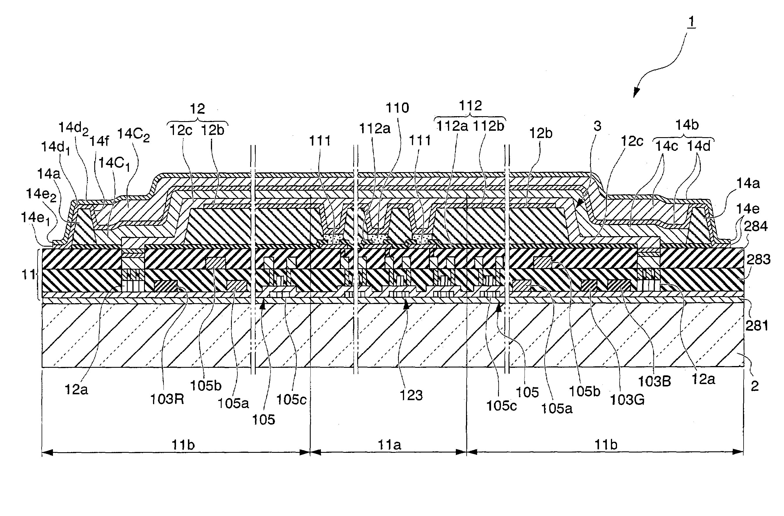
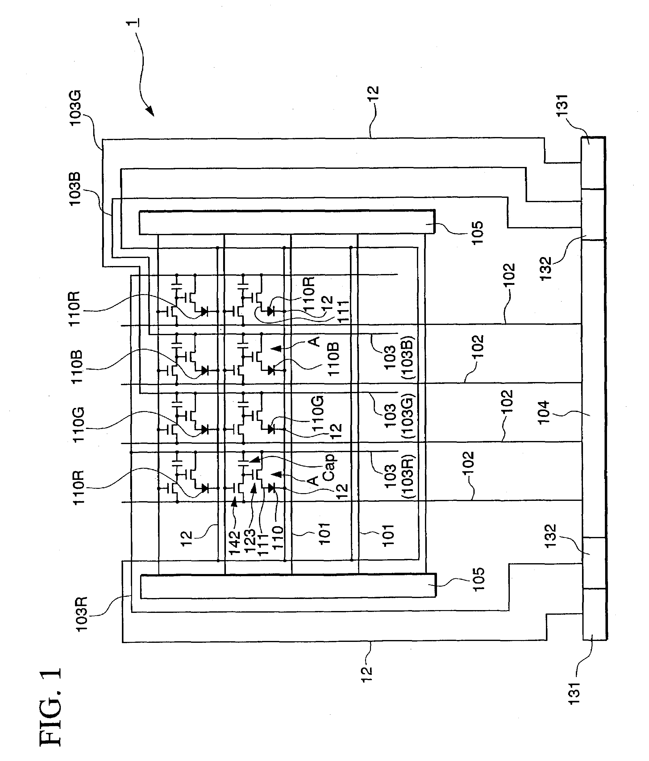
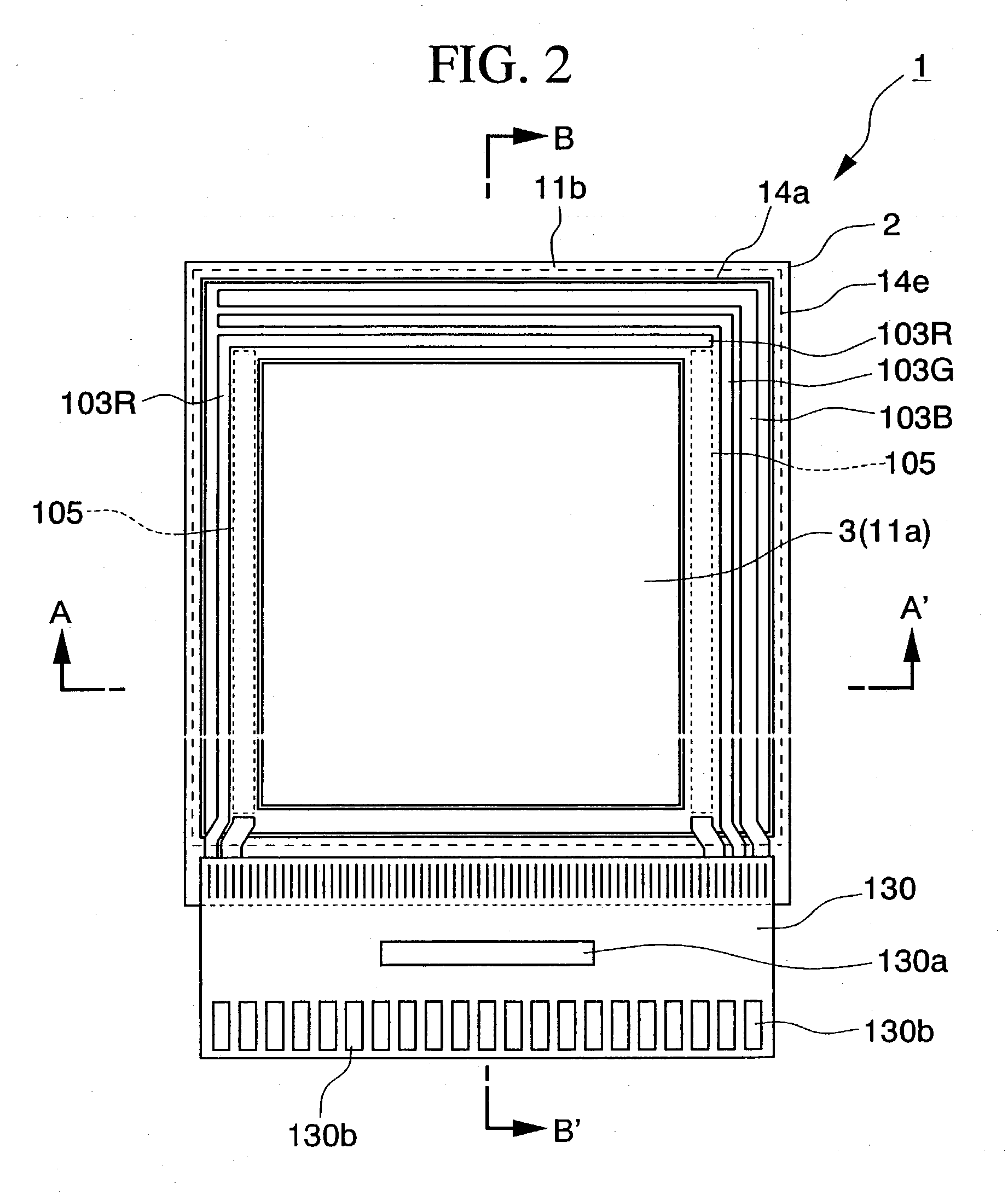
[0089]FIG. 1 is a schematic plan view showing the wiring configuration of a display device (an organic EL display device) according to the first embodiment of the present invention. The display device 1 shown in FIG. 1 is an organic EL display device of an active matrix type in which thin film transistors (TFTs...

second embodiment

[0146]Next, a second embodiment will be explained below with reference to FIG. 13. FIG. 13 is a cross-sectional view showing the major portion of the sealing structure of a display device 201.

[0147]The elements of the display device 201 shown in FIG. 13 that are common to those of the display device I of the first embodiment shown in FIGS. 1 to 4 will be provided with the same reference symbols, and explanation therefor will be simplified or omitted.

[0148]As shown in FIG. 13, the display device 201 of the present embodiment is provided with a plurality of peripheral banks (blocking regions) 214a1, 213a2, and 214a3. The innermost peripheral bank is indicated by reference symbol 214a1, another peripheral bank indicated by reference symbol 214a2 is formed outside the peripheral bank layer 214a1, and a further peripheral bank layer 214a3 is formed outside the peripheral bank layer 214a2.

[0149]The distances “d” between the peripheral bank layer 214a1 and the peripheral bank layer 214a2, ...

third embodiment

[0173]Next, a third embodiment will be explained below with reference to FIG. 16. FIG. 16 is a cross-sectional view showing the major portion of the sealing structure of a display device 301.

[0174]The elements of the display device 301 shown in FIG. 16 that are common to those of the display device 1 of the first embodiment shown in FIGS. 1 to 4 will be provided with the same reference symbols, and explanation therefor will be simplified or omitted.

[0175]As shown in FIG. 16, in the display device 301 of the present embodiment, there are formed a plurality of liquid-repelling regions (blocking regions) 314a1, 314a2, and 3l4a3 on the peripheral area of the inorganic bank layer 112a (of the substrate 2). More specifically, the innermost liquid-repelling region is indicated by reference symbol 314a1, another liquid-repelling region indicated by reference symbol 314a2 is formed outside the liquid-repelling region 314a1, and a further liquid-repelling region 314a3 is formed outside the li...


PUM


Abstract

A sealing structure having a barrier membrane, with which the overall thickness of a display device can be reduced while ensuring sufficient barrier properties against water and oxygen so as to prevent deterioration of luminous layers. The sealing structure includes a multi-layered resin membrane for sealing an electronic element section disposed on a substrate, which is formed by alternately depositing flattening resin layers and barrier layers on the substrate. The flattening resin layers are formed inside a blocking region surrounding the electronic element section. A display device having the sealing structure, an electronic apparatus having the display device, and a fabrication method for the display device are also disclosed.

Description

BACKGROUND OF THE INVENTION[0001]1. Field of the Invention[0002]The present invention relates to a sealing structure for an electronic element section such as a display element, a semiconductor circuit element, etc., and more specifically, the present invention relates to a sealing structure with a barrier membrane for a display device, an electronic apparatus, and an electronic element section, as well as to a fabrication method therefor. The description of the present invention herein specifically pertains to an organic EL display device as an example of preferred applications; however, the present invention is not limited to the organic EL display device.[0003]2. Background Art[0004]In recent years, color display devices, which contain a plurality of display elements each of which comprises a pair of electrodes and active layers, such as a hole-injection layer / transportation layer, a luminous layer, etc., being sandwiched between the pair of electrodes, have been developed, and s...

Claims


Application Information

Patent Timeline
IPC IPC(8): H05B33/04H01L27/32H01L51/52
CPCH05B33/04H01L27/3246H01L51/5256H01L27/3244Y10S428/917H10K59/122H10K59/12H10K50/8445
Inventor IMAMURA, YOICHI
Owner SEIKO EPSON CORP
Why Eureka
Try Eureka