Exposure apparatus and device manufacturing method

a technology of exposure apparatus and manufacturing method, which is applied in the direction of photomechanical apparatus, printers, instruments, etc., can solve the problems of deterioration in imaging performance, further reduction of exposure light amount, and deterioration of imaging performance, so as to reduce the adhesion of contaminant, improve imaging performance, and reduce the effect of exposure light amoun

Inactive Publication Date: 2006-09-19
CANON KK
View PDF6 Cites 4 Cited by
  • Summary
  • Abstract
  • Description
  • Claims
  • Application Information

AI Technical Summary

Benefits of technology

[0015]It is, therefor, an exemplified object of the present invention to provide an exposure apparatus capable of suppressing adherence of a contaminant to an optical element surface, and realizing a high throughput and a satisfactory imaging performance.
[0017]According to the present invention, it is possible to provide an exposure apparatus capable of suppressing adherence of a contaminant to an optical element surface, and realizing a high throughput and a satisfactory imaging performance.

Problems solved by technology

If a product (ammonium sulfate or silicon dioxide) generated by the photochemical reaction adheres to an optical element, the surface of the optical element is fogged, leading to not only a further reduction in exposure light amount, but also, deterioration in imaging performance.
If the motor 1800 has a gas-producing property, an exhaust gas EG adheres to the lens unit 1200 due to a photochemical reaction, leading to deterioration in imaging performance, as well as a reduction in exposure light amount.
However, with a structure of the aforementioned conventional exposure apparatus, it becomes more difficult to sufficiently suppress a reduction in throughput and deterioration in imaging performance due to contamination of an optical element, as the wavelength of the exposure light becomes shortened.
Although the motor is configured so as to minimize the exhaust gas production as mentioned above, it is impossible to use undesirable materials to maintain performance of the motor.
However, the structure of the conventional exposure apparatus requires a long time to reach such a water or an oxygen content so as to satisfy a required optical performance.
This is supposedly because it takes much time to purge with an inert gas the air having intruded and accumulated in the inside of the motor or in minute gaps of a lens holding mechanism or other such mechanisms.

Method used


Image

  • Exposure apparatus and device manufacturing method
  • Exposure apparatus and device manufacturing method
  • Exposure apparatus and device manufacturing method

Examples


Embodiment Construction

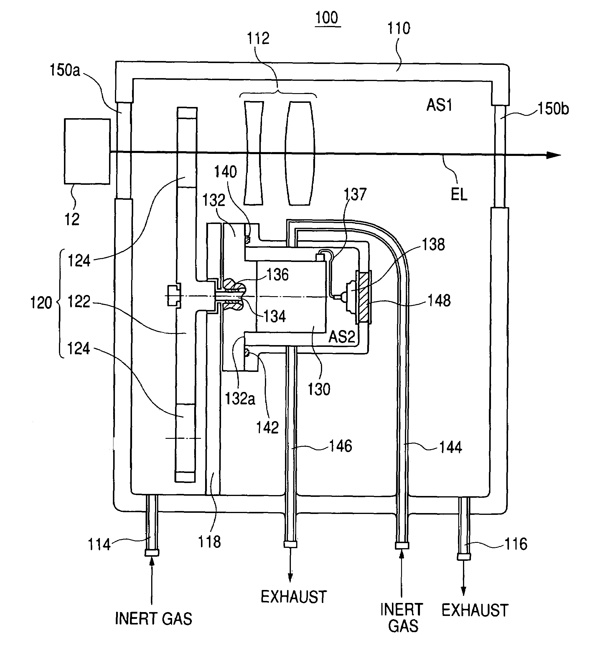
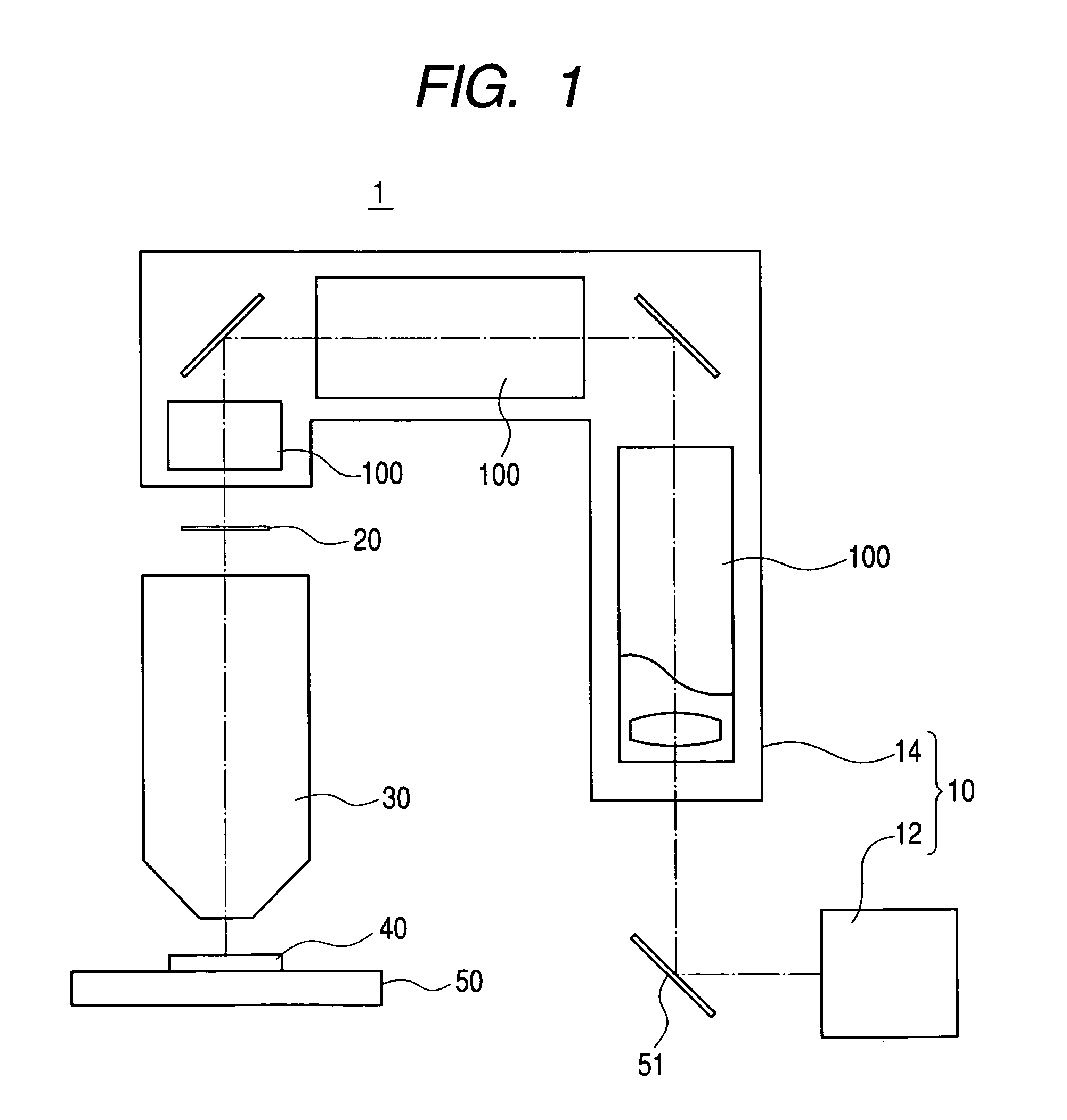
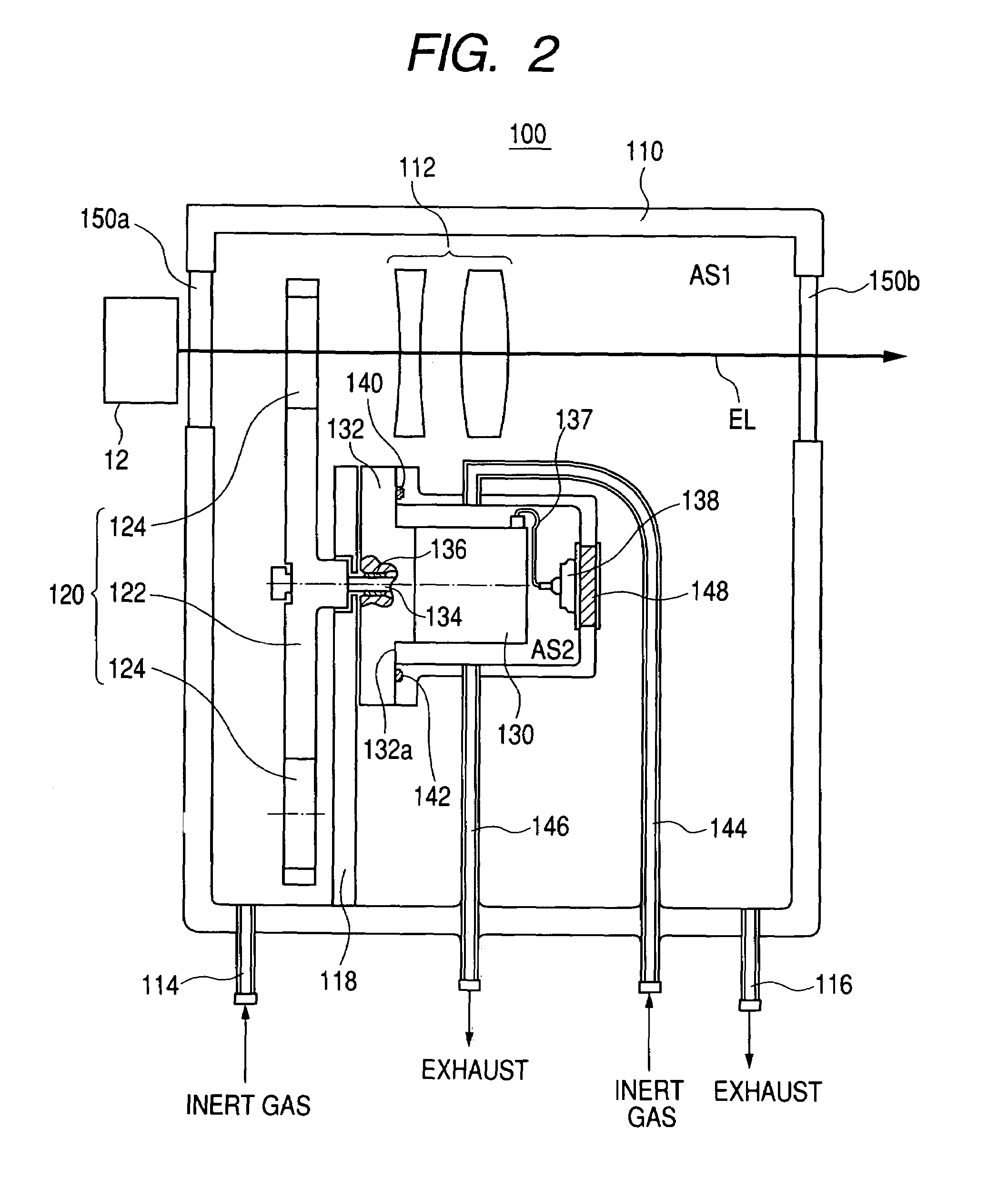
[0029]Hereinafter, an exposure apparatus according to an embodiment of the present invention will be described with reference to the accompanying drawings. Note that the same reference symbols are assigned to the same members throughout the drawings, and a repetitive explanation is omitted. Here, FIG. 1 is a schematic sectional view showing a structure of an exposure apparatus 1 according to the embodiment of the present invention.

[0030]As shown in FIG. 1, the exposure apparatus 1 includes an illuminator 10 for illuminating a reticle 20 having a circuit pattern formed thereon; a projection optical system 30 for projecting a diffraction ray diffracted by the reticle pattern onto an object to be processed (plate) 40; and a stage 50 for supporting the object to be processed 40.

[0031]The exposure apparatus 1 serves as a projection exposure apparatus for projecting the circuit pattern formed on the reticle 20 to the plate 40 through exposure, by using a step-and-scan process or a step-an...


PUM

PropertyMeasurementUnit
wavelengthaaaaaaaaaa

Abstract

An exposure apparatus for exposing a substrate to light from a light source via a reticle. The exposure apparatus includes an optical system configured to expose the substrate to light from the light source via the reticle, and has a first optical element, a motor configured to move the first optical element, a first housing accommodating at least the first optical element and the motor, a second housing accommodated in the first housing, accommodating at least a part of the motor, and configured to isolate the part of the motor from the first optical element, a first exhaust system configured to exhaust a first space between the first housing and the second housing, and a second exhaust system configured to exhaust a second space in the second housing.

Description

BACKGROUND OF THE INVENTION[0001]1. Field of the Invention[0002]The present invention relates generally to an exposure apparatus. In particular, the invention relates to an exposure apparatus used for exposing an object to be processed (substrate), such as a single crystal substrate for a semiconductor device or a glass substrate for a liquid crystal display (LCD). The present invention is suitable, for example, for an exposure apparatus using a light beam having a wavelength not longer than 200 nm.[0003]2. Related Background Art[0004]There is an increasing demand for miniaturization of a semiconductor element installed in an electronic device in order to respond to recent requests for reduction in size and thickness of the electronic device. Up to now, a projection exposure apparatus has been used in a lithography (printing) process for manufacturing a semiconductor element, the apparatus projecting and transferring a circuit pattern drawn on a reticle or mask (in this application,...

Claims


Application Information

Patent Timeline
Patent Type & Authority Patents(United States)
IPC IPC(8): G03B27/42G03B27/52G03F7/20H01L21/027
CPCG03F7/70808G03F7/70933G03F7/70916
Inventor TOMINAGA, YASUTERU
Owner CANON KK
Why Eureka
Try Eureka