Substrate for pre-soldering material and fabrication method thereof

a technology of pre-soldering material and substrate, which is applied in the direction of printed circuit manufacturing, printed circuit assembling, solid-state devices, etc., can solve the problems of difficult depositing of pre-soldering material, and achieve the effect of strengthening pre-soldering joint and preventing the reduction of conductive pad area

Inactive Publication Date: 2006-09-26
PHOENIX PRECISION TECH CORP
View PDF4 Cites 39 Cited by
  • Summary
  • Abstract
  • Description
  • Claims
  • Application Information

AI Technical Summary

Benefits of technology

[0013]Another objective of the present invention is to provide a substrate for a pre-soldering material and a method for fabricating the same, whereby a contact area between the conductive pads and the deposited soldering material is increased to strengthen pre-soldering joint.
[0014]A further objective of the present invention is to provide a substrate for a pre-soldering material and a method for fabricating the same so as to prevent reduction of the conductive pad area exposed by the insulating layer. As a result, this resolves subsequent bump alignment problem and difficulty in depositing the pre-soldering material on the conductive pads.
[0018]In contrast to the conventional method, the upper surface of the conductive pad is exposed from the insulating layer in the present invention. Therefore, a larger area of the conductive pad is provided for forming the pre-soldering material. Without forming the insulating layer to occupy space which is between chip and its package substrate, the present invention can reduce the amount of pre-soldering material required as well as the thickness of the package substrate, making the semiconductor package lighter and more compact, while the fabrication cost is minimized. And as the contact area between the conductive pads and the deposited pre-soldering material is increased, the bonding strength for the pre-soldering material is enhanced.

Problems solved by technology

As a result, this resolves subsequent bump alignment problem and difficulty in depositing the pre-soldering material on the conductive pads.

Method used


Image

  • Substrate for pre-soldering material and fabrication method thereof
  • Substrate for pre-soldering material and fabrication method thereof
  • Substrate for pre-soldering material and fabrication method thereof

Examples


Embodiment Construction

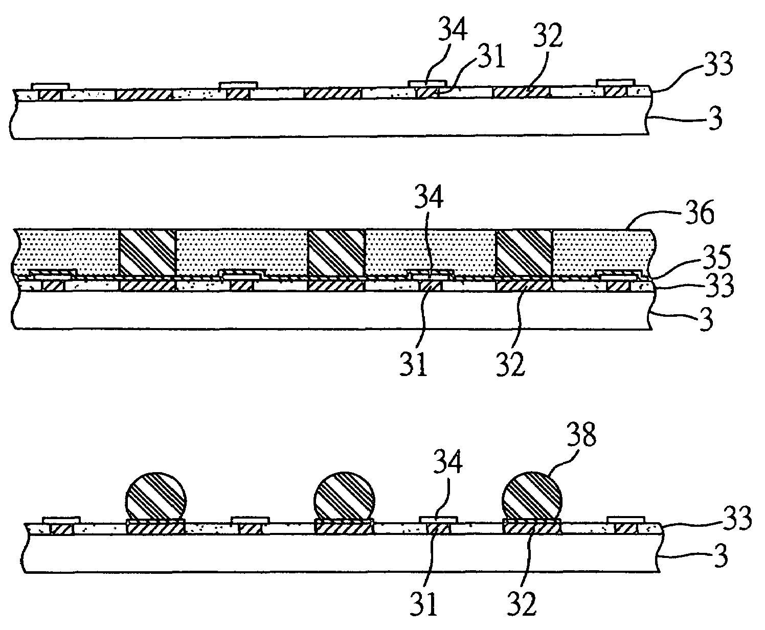
[0029]A substrate for pre-soldering material and a fabrication method thereof are illustrated in the diagrams below. It should be noted here that the diagrams below are schematic diagrams illustrating only basic construction of the present invention, and only components relevant to the present invention are illustrated. So, the actual layout for the components can be more complicated in terms of their number, shape, and ratio.

[0030]FIGS. 3A through to 3I are schematic cross-sectional diagrams illustrating method for fabricating the substrate formed with pre-soldering material according to one preferred embodiment of the present invention.

[0031]Referring to FIG. 3A, a substrate 3 is provided. The substrate 3 has a surface formed with a plurality of conductive pads 32. A plurality of conductive traces 31 may also be formed on the surface of the substrate to electrically connect with the conductive pads 32. As the method for forming the conductive pads and conductive traces is well kno...


PUM


Abstract

A substrate for a pre-soldering material and a fabrication method of the substrate are proposed. The substrate having at least one surface formed with a plurality of conductive pads is provided. An insulating layer is formed over the surface of the substrate in such a way that a top surface of each of the conductive pads is exposed. Next, a conductive film and a resist layer are formed in sequence on the insulating layer and the conductive pads, wherein a plurality of openings are formed in the resist layer to expose a part of the conductive film above the conductive pad. Then, a pre-soldering material is deposited over the conductive pad by stencil printing or electroplating process.

Description

BACKGROUND OF THE INVENTION[0001]1. Field of the Invention[0002]The invention relates to substrates for pre-soldering materials and fabrication methods thereof, and more particularly, to a substrate having exposed conductive pads thereon for use with a pre-soldering material applied by electroplating or stencil printing process and a fabrication method of the substrate.[0003]2. Description of the Related Art[0004]In the early 60, IBM has introduced a flip chip package technology characterized by having solder bumps to connect the semiconductor chip and the substrate, instead of having the gold wire as in the typical wire bonding technique. The flip chip package technology has benefits in terms of increasing package integration, and reducing package device size, while a long metal wire is not required in the flip chip package technology in order to enhance electrical function of the device. For many years, manufacturers have adopted a thermal soldering on the ceramic substrate in a t...

Claims


Application Information

Patent Timeline
Patent Type & Authority Patents(United States)
IPC IPC(8): H01L21/44H01L21/60H05K3/34
CPCH01L24/11H05K3/3473H01L24/81H01L2224/0401H01L2224/11462H01L2224/1147H01L2224/11849H01L2224/13099H01L2224/13144H01L2224/13147H01L2224/16H01L2224/1607H01L2224/81801H01L2224/83102H01L2224/92125H01L2924/01012H01L2924/01015H01L2924/01022H01L2924/01029H01L2924/0103H01L2924/0104H01L2924/01046H01L2924/01047H01L2924/01049H01L2924/01051H01L2924/01052H01L2924/01075H01L2924/01078H01L2924/01079H01L2924/01082H01L2924/14H01L2924/1433H01L2924/15311H05K3/3484H05K2203/054H01L2924/01024H01L2924/01033H01L2924/0105H01L2924/014H01L2924/01006H01L2924/0002H01L2224/11334H01L2224/16225H01L2924/10253H01L2224/05568H01L2224/81191H01L2224/81193H01L2224/81192H01L2924/00H01L2224/05552H01L2924/351H01L2924/15787H01L2924/12042H05K3/3485
Inventor HSU, SHIH-PINGHU, CHU-CHIN
Owner PHOENIX PRECISION TECH CORP
Why Eureka
Try Eureka