Semiconductor memory device, a sector-address conversion circuit, an address-conversion method, and operation method of the semiconductor memory device

a semiconductor memory and sector address technology, applied in the direction of memory address formation, micro-instruction address formation, allocation/relocation, etc., can solve the problems of difficult rewriting of memory devices, and inability to be easily performed

Inactive Publication Date: 2006-09-26
SOCIONEXT INC
View PDF7 Cites 4 Cited by
  • Summary
  • Abstract
  • Description
  • Claims
  • Application Information

AI Technical Summary

Benefits of technology

[0019]The present invention enables easy rewriting of a memory while maintaining contents of another memory by splitting a semiconductor memory device (for example, a flash memory) into a plurality of areas (for example, banks) wherein the plurality of the areas accommodate a plurality of small sectors in the highest or the lowest physical address in each area or in a series of a plurality of the physical addresses containing the highest or the lowest physical address in the area, respectively.
[0023]In these manners, a sector address can be converted for a desired boot block type easily.

Problems solved by technology

However, rewriting of the data within the same system and the like always requires to use the same boot block type from design restrictions, and rewriting between memory devices with different boot block types has a problem that it cannot be easily performed.
However, a problem with this type is that address areas of the boot block differ (e.g. a bank or some banks are the top boot block type and the other banks are the bottom boot block type), causing difficulties in rewriting the memory device.

Method used


Image

  • Semiconductor memory device, a sector-address conversion circuit, an address-conversion method, and operation method of the semiconductor memory device
  • Semiconductor memory device, a sector-address conversion circuit, an address-conversion method, and operation method of the semiconductor memory device
  • Semiconductor memory device, a sector-address conversion circuit, an address-conversion method, and operation method of the semiconductor memory device

Examples


Embodiment Construction

[0041]In the following, an embodiment of the present invention will be described with reference to the accompanying drawings.

[0042]First, the principle of the sector address conversion of the memory device of this invention will be described with reference to FIGS. 4A, 4B and 4C and FIG. 5.

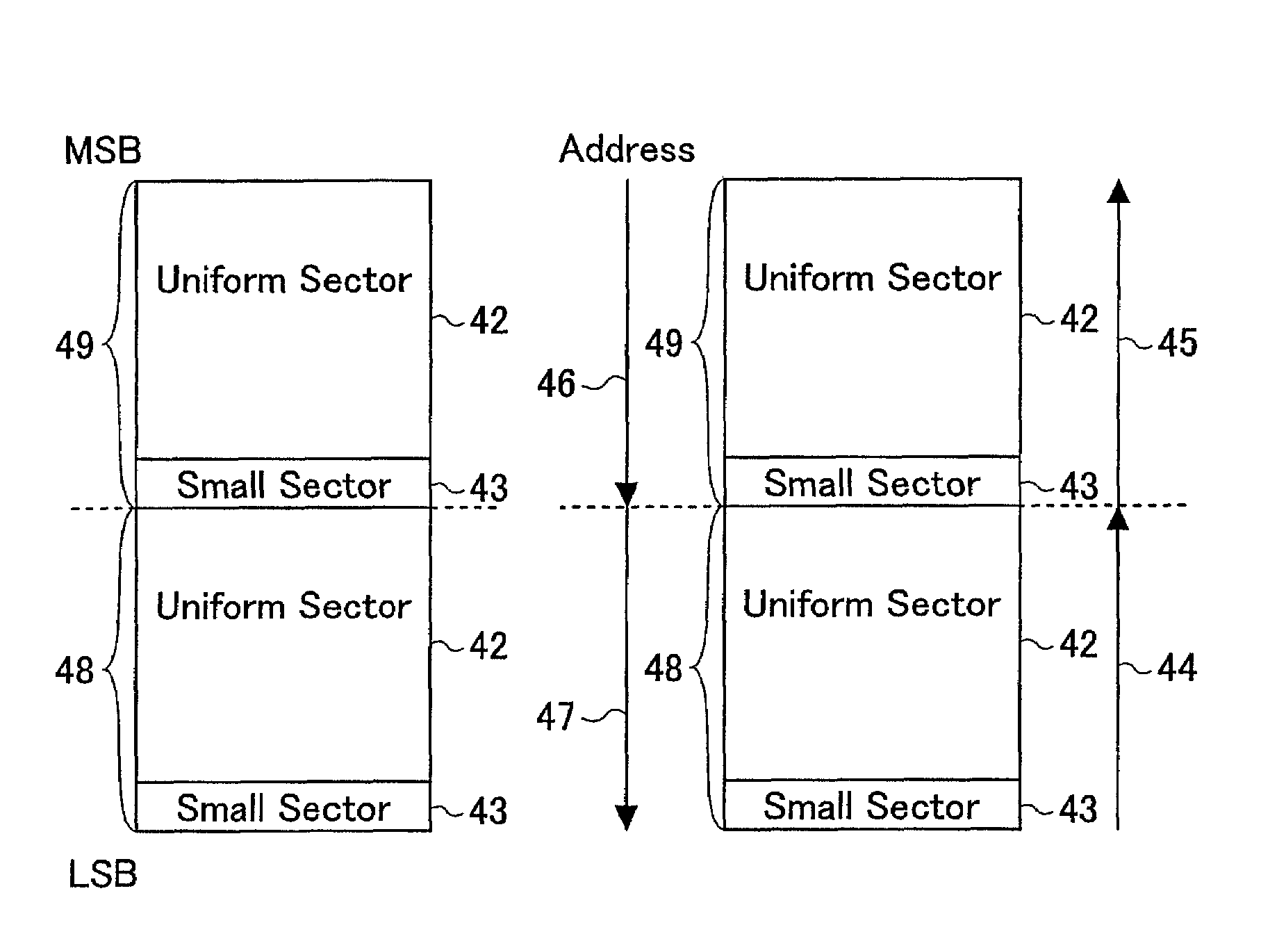
[0043]As shown in FIG. 4A, a sector address from the outside is inputted into a sector-address conversion circuit 40. By the sector-address conversion circuit 40, the address is converted into a sector address of the internal address, and a memory cell array (memory device) is accessed through an address decoder circuit 41.

[0044]The memory device can be accessed from the outside as a top boot type or a bottom boot type memory device as required by the sector-address conversion circuit 40, regardless of whether the memory device is (originally) a top boot type or a bottom boot type.

[0045]The memory device shown in FIG. 4B has two banks 48 and 49, each of which includes a uniform sector 42 and a sma...


PUM


Abstract

The present invention aims at providing a semiconductor memory device that can be operational in a desired boot block mode, regardless of the original boot block type of the device, by facilitating rewriting of the memory device. A sector address from an outside source is inputted into a sector-address conversion circuit, which converts the sector address into an internal address, and a memory cell array is accessed through an address decoder circuit. Suppose that each of banks of the memory device is configured as a bottom boot type. By converting the sector address by the sector-address conversion circuit such that the sector-address now appears to the outside in the reverse order, each of the banks now functions as a top boot type.

Description

BACKGROUND OF THE INVENTION[0001]1. Field of the Invention[0002]This invention relates to a semiconductor memory device, a sector-address conversion circuit, an address-conversion method, and an operation method of the semiconductor memory device.[0003]2. Description of the Related Art[0004]Various kinds of memory devices including a flash memory are known. Generally, the first operation at starting of a system, reset operation and the like is performed by reading a read-only boot program and the like from a memory device.[0005]Conventionally, a boot block used as an object for starting of a system occupies a small sector in a memory device, and is located in the high end or the low end of sector addresses (physical addresses) of the memory device (a bottom boot type or a top boot type, respectively, and called a boot block type) according to a requirement specification of the system. The two types are marketed as distinctly individual products.[0006]FIG. 1A shows the top boot type ...

Claims


Application Information

Patent Timeline
Patent Type & Authority Patents(United States)
IPC IPC(8): G06F12/00G11C16/02G06F9/445G06F11/00G06F12/02G06F12/06
CPCG06F9/4403
Inventor SHOJI, HARUO
Owner SOCIONEXT INC
Why Eureka
Try Eureka