

SRAM circuit based on pnpn structure and its reading and writing method
A circuit and voltage technology, which is applied to the SRAM circuit based on PNPN structure and its reading and writing field, can solve the problems of different electrical characteristics, and the SRAM reading and writing circuit cannot be applied to the storage unit, so as to improve the overall performance of the circuit, fast reading speed, The effect of occupying a small area
- Summary
- Abstract
- Description
- Claims
- Application Information
AI Technical Summary
Problems solved by technology
Method used
Image

Examples
Embodiment Construction
[0031] The features and technical effects of the technical solution of the present invention are described in detail below with reference to the accompanying drawings and in combination with schematic embodiments, and methods are disclosed. It should be pointed out that similar reference numerals represent similar structures, and the terms "first", "second", "upper", "lower" and the like used in this application can be used to modify various device structures or process steps . These modifications do not imply spatial, sequential or hierarchical relationships of the modified device structures or process steps unless otherwise specified.
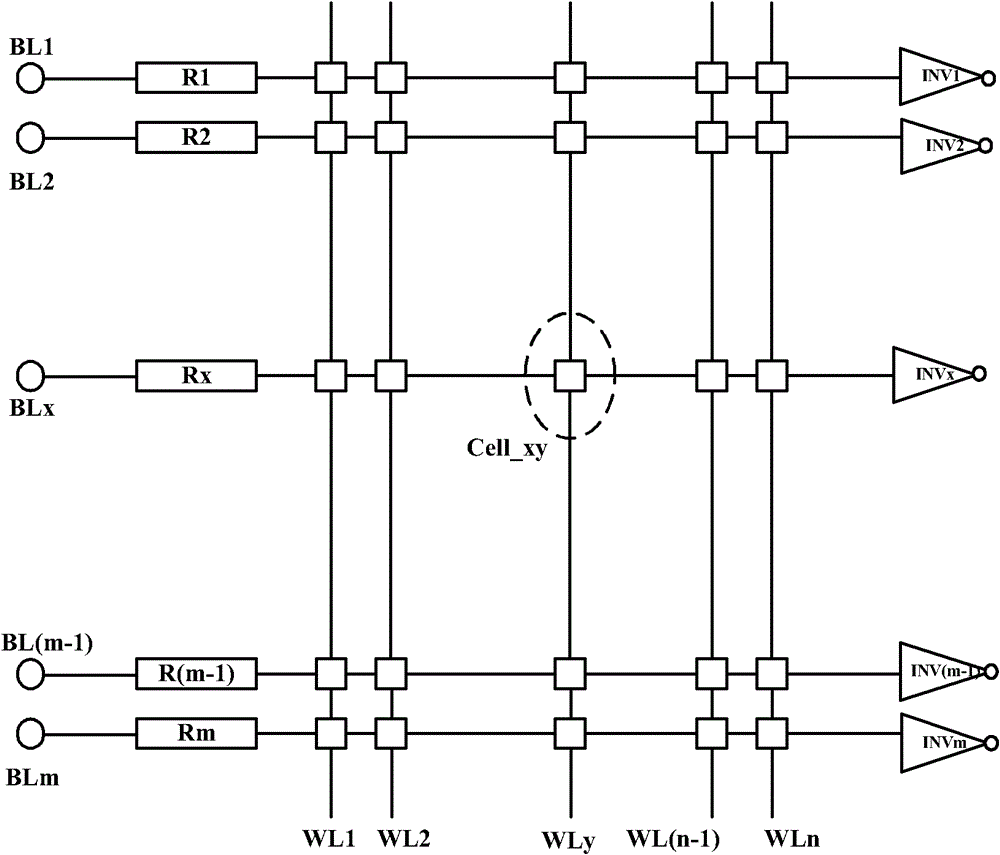
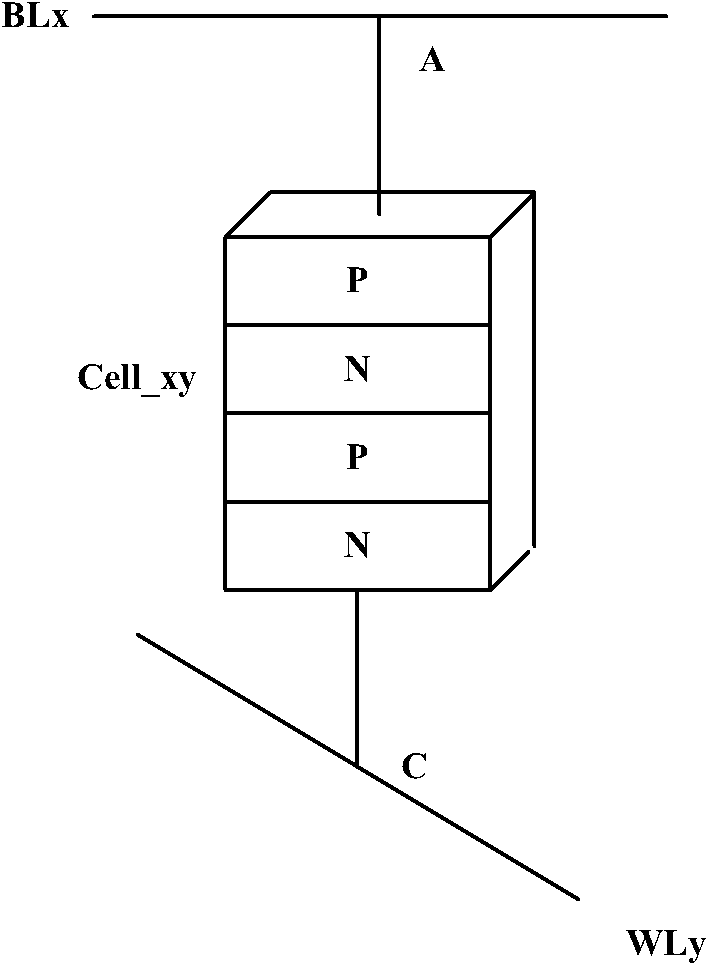
[0032] refer to Figure 1A , shows a schematic circuit diagram of an SRAM based on a PNPN structure according to an embodiment of the present invention, including an m×n SRAM array of m rows and n columns, which can store m×n bytes (byte), which also includes BL1, BL2 , BLx, BL(m-1), BLm and other bit lines, and multiple word lines such as W...
PUM
 Abstract
Description
Claims
Application Information