Mask pattern inspecting method, inspection apparatus, inspecting data used therein and inspecting data generating method

Inactive Publication Date: 2006-09-26
SOCIONEXT INC
View PDF7 Cites 7 Cited by
  • Summary
  • Abstract
  • Description
  • Claims
  • Application Information

AI Technical Summary

Benefits of technology

[0035]In consideration of the actual circumstances, the invention has been made and has an obj

Problems solved by technology

Even if a mask pattern region is excessively large or small, the accuracy in the etching is reduced.
Moreover, the formation of a diffusion layer also has the same problems.
If an ion implantation region for forming the diffusion layer is too small, the concentration of the ion is generated so that a desirable diffusion profile cannot be obtained.
Consequently, there is a problem in that a time (TAT) required from an order to a completion is increased.
Moreover, the photomask is expensive.
Therefore, a sudden rise in a cost caused by the necessity of a large number of photomask blanks for carrying out the manufacture again is also a serious problem.
In the case in which the pattern density of a wiring layer to be a lower layer is low and there is a region including a pattern having a predetermined are

Method used


Image

  • Mask pattern inspecting method, inspection apparatus, inspecting data used therein and inspecting data generating method
  • Mask pattern inspecting method, inspection apparatus, inspecting data used therein and inspecting data generating method
  • Mask pattern inspecting method, inspection apparatus, inspecting data used therein and inspecting data generating method

Examples


Example

First Embodiment

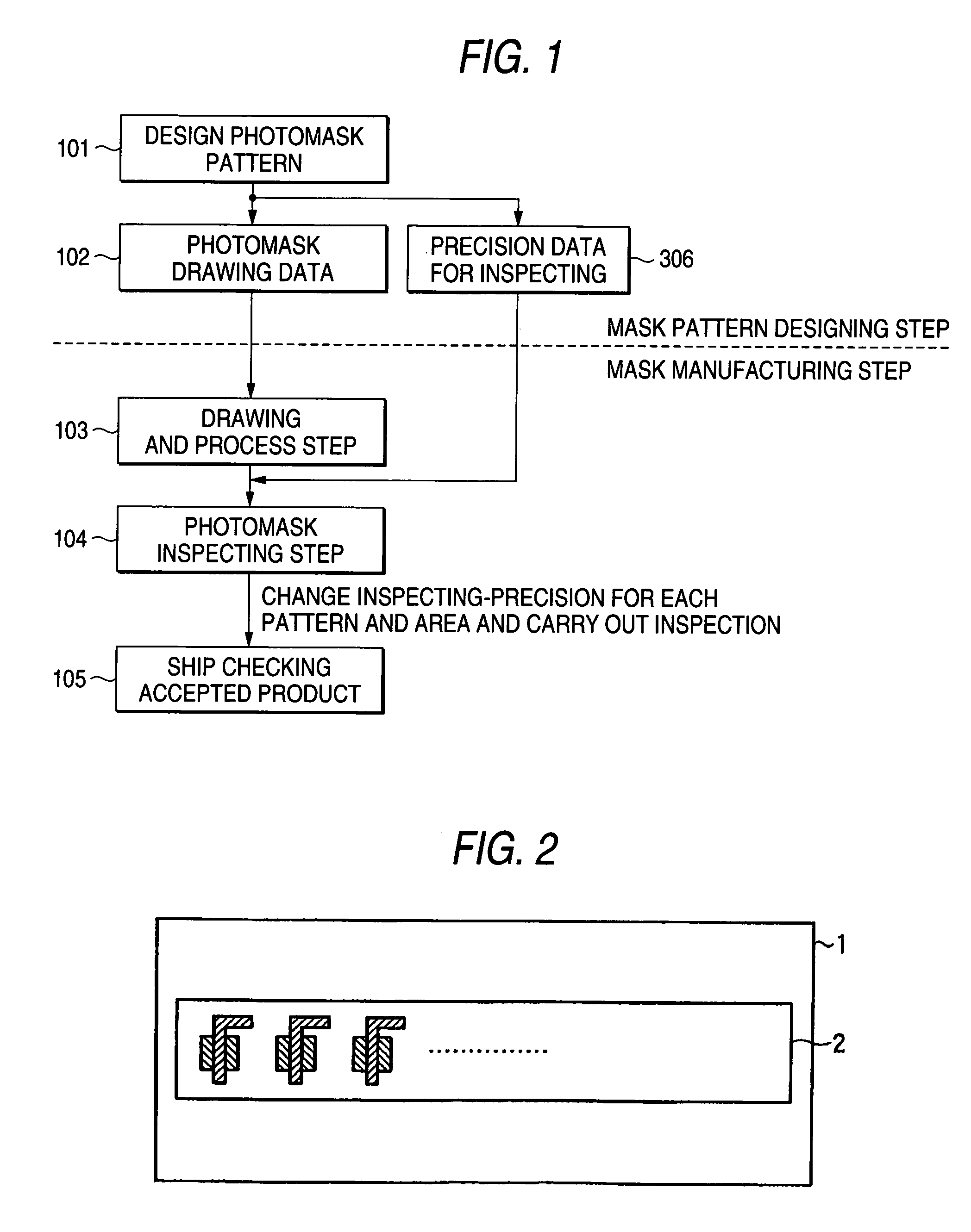
[0098]In a photomask inspecting method according to the invention, when inspecting a photomask for a semiconductor integrated circuit formed based on drawing pattern data, a drawing pattern of the semiconductor integrated circuit is classified into a plurality of ranks in accordance with a predetermined reference and is thus extracted, inspecting accuracy is determined for each of the ranks, and quality of the photomask is decided depending on whether the determined inspecting accuracy is satisfied.

[0099]FIG. 1 shows a photomask inspecting flow according to the embodiment. While constant accuracy is specified from a design rule over a whole photomask in a conventional inspecting flow, inspecting accuracy data 306 are separately formed based on a photomask pattern obtained at a photomask pattern design step 101 and the inspection of the photomask is executed based on an inspecting accuracy reference set for each pattern area on the basis of the inspecting accuracy dat...

Example

Second Embodiment

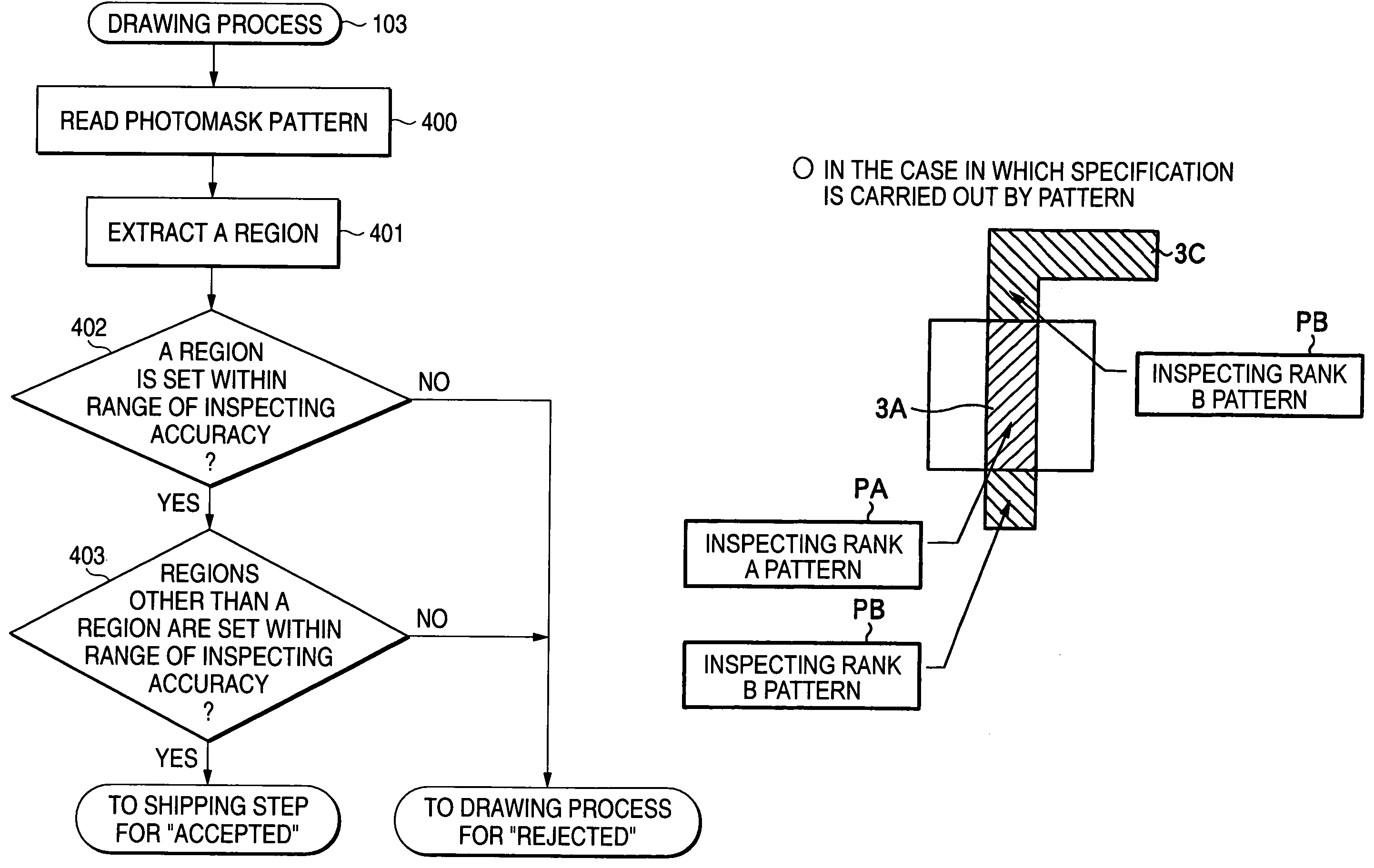
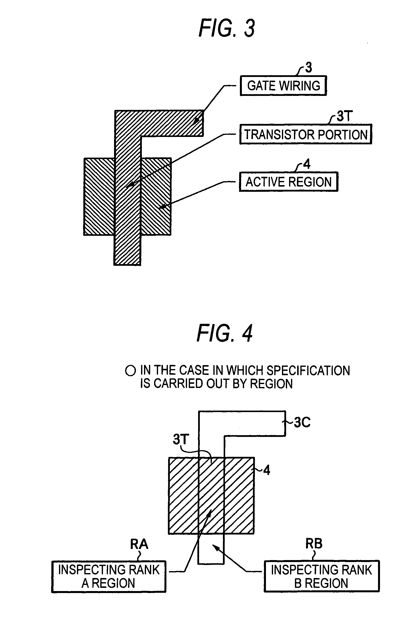
[0118]While the classification of the inspecting rank is specified for each region in the first embodiment, it may be specified for each pattern.

[0119]More specifically, as shown in FIG. 6, only the gate pattern of a region constituting a true gate region in the gate wiring 3 is set to be an An inspecting rank pattern PA corresponding to an inspecting rank with high accuracy, and the other patterns are set to be a B inspecting rank pattern PB corresponding to a lower rank.

[0120]Also in this case, at a photomask inspecting step, the embodiment is the same as the first embodiment except that a method of extracting inspecting data and an inspecting reference are different.

[0121]By this method, similarly, a channel length can reliably be maintained and a photomask of high quality can be implemented in a short time at a low cost in the same manner as in the first embodiment. By this method, particularly, it is possible to produce an advantage that data indicative of an i...

Example

Third Embodiment

[0122]While the classification of the inspecting rank is specified for each region in the first embodiment, moreover, it may be specified by the edge of a pattern.

[0123]More specifically, as shown in FIG. 7, only the gate pattern edge of a region constituting a true gate region in a gate wiring 3 is set to be an An inspecting rank edge EA corresponding to an inspecting rank with high accuracy, and the other patterns are set to be a B inspecting rank edge EB corresponding to a lower rank.

[0124]Also in this case, the embodiment is the same as the first embodiment except that a method of extracting inspecting data and an inspecting reference are different at a photomask inspecting step.

[0125]According to this method, it is possible to obtain an advantage that a deciding rank can be set every edge as compared with the first embodiment.


PUM


Abstract

A method of inspecting a photomask for a semiconductor integrated circuit formed based on drawing pattern data, includes the steps of classifying a drawing pattern of the semiconductor integrated circuit into a plurality of ranks in accordance with a predetermined reference and extracting the same, determining inspecting accuracy for each of the ranks, and deciding quality of the photomask depending on whether the determined inspecting accuracy is satisfied.

Description

[0001]The present application is based on Japanese Patent Application No. 2002-342304, which is incorporated herein by reference.BACKGROUND OF THE INVENTION[0002]1. Field of the Invention[0003]The present invention relates to a method of inspecting a mask pattern, an inspection apparatus, inspecting data used therein and a method of generating the inspecting data, and more particularly to the extraction and inspection of inspecting accuracy data in a process for inspecting a photomask.[0004]2. Description of the Related Art[0005]In recent years, a semiconductor integrated circuit device (hereinafter referred to as an LSI) in each product is evaluated as a key device, and an increase in the scale and speed of the LSI has been required in order to maintain the competitiveness of the product. A fine process is necessary with the microfabrication of an element and an increase in integration.[0006]Under the circumstances, process conditions have been increasingly restricted in order to f...

Claims


Application Information

Patent Timeline
IPC IPC(8): G06F17/50G03F1/84G03F7/20G06T7/00
CPCG03F1/84G06T7/0004G03F7/70616G06T2207/30148
Inventor TOKUNAGA, SHINYATSUJIKAWA, HIROYUKITANIMOTO, TADASHI
Owner SOCIONEXT INC
Why Eureka
Try Eureka