Multi-layered electrophotographic positively charged organic photoconductor and manufacturing method thereof

Inactive Publication Date: 2006-10-03
S PRINTING SOLUTION CO LTD
View PDF20 Cites 8 Cited by
  • Summary
  • Abstract
  • Description
  • Claims
  • Application Information

AI Technical Summary

Benefits of technology

[0011]Therefore, the present invention has been made in view of the above and/or other problems, and it is an aspect of the present invention to provide a multi-layered electrophotographic positively charged organic photoconductor with improved proper

Problems solved by technology

Otherwise, the charge generating layer may be worn away by friction with a toner and a cleaning blade.
However, the multi-layered positively charged organic photoconductor has a disadvantage in that when a composition to form a charge generating layer is coated on a charge transport layer, an organic solvent in the composition may dissolve a part of the charge transport layer that is disposed under the charge generating layer.
Consequently, the thickness of the charge transport layer may change, or substances making up the charge transport layer may be dissolved, which may cause a reduc

Method used


Image

  • Multi-layered electrophotographic positively charged organic photoconductor and manufacturing method thereof
  • Multi-layered electrophotographic positively charged organic photoconductor and manufacturing method thereof
  • Multi-layered electrophotographic positively charged organic photoconductor and manufacturing method thereof

Examples


example 1

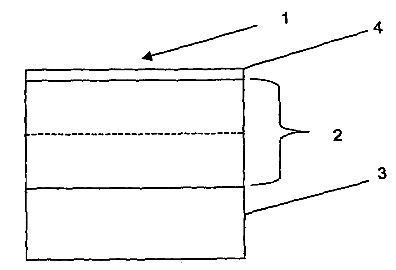
[0099]1.15 g of a hole transport material of the formula (V) and 1.15 g of a hydrazone compound of the formula (IX), 0.23 g of polyethyleneterephthalate copolymer (O-PET4-50, supplied by KANEBO, LTD., Japan) and 2.07 g of polycarbonate (PCZ200, supplied by MITSUBISHI CHEMCIAL CORP., Japan) were dissolved in 15.4 g of tetrahydrofuran and filtered through a filter paper with a pore size of 1 μm. Then, the filtrate was coated on an aluminum drum at a rate of 300 mm / min in a ring coating apparatus and dried in an oven at 110 C for 15 minutes to form a charge transport layer. The charge transport layer thus obtained has a thickness of about 8 μm.

[0100]Then, 0.84 g of polyvinylbutyral (BX-1, SEKISHI CO., LTD., Japan) was dissolved in 17.2 g of ethanol to obtain a solution. 1.96 g of TiOPc (titanyloxy phthalocyanine), as a charge generating material, was added the solution. The resulting solution was milled for 1 hour in an attritor type miller to obtain a dispersion. Separately, 0.08 g of...

example 2

[0103]A multi-layered electrophotographic positively charged organic photoconductor was formed by repeating the procedure of Example 1 except that 0.16 g of a compound of the formula (XII) was used as the hole transport material to prepare the composition to form a charge generating layer.


PUM


Abstract

A multi-layered electrophotographic positively charged organic photoconductor includes a conductive substrate, a charge transport layer formed on the conductive substrate, and a charge generating layer formed on the charge transport layer. A composition to form the charge transport layer includes at least one hole transport material, a binder resin and an organic solvent, and a composition to form the charge generating layer includes a charge generating material, a binder resin, an organic solvent and a hole transport material. An organic photoconductor has improved static electrical properties by controlling interfacial conditions of the charge transport layer and the charge generating layer. The charge generating layer may be readily coated on the charge transport layer. In addition, the organic photoconductor has excellent electric properties such as an improved sensitivity and a low discharge voltage.

Description

CROSS-REFERENCE TO RELATED APPLICATIONS[0001]This application claims the benefit of Korean Application No. 2002-60013, filed Oct. 2, 2002, in the Korean Intellectual Property Office, the disclosure of which is incorporated herein by reference.BACKGROUND OF THE INVENTION[0002]1. Field of the Invention[0003]The present invention relates to a multi-layered electrophotographic positively charged organic photoconductor, and more particularly, a multi-layered electrophotographic positively charged organic photoconductor with superior electric properties, such as an improved sensitivity and a reduced discharge voltage in which a composition for forming a charge generating layer comprises a hole transport material, wherein charges may be readily injected to a charge transport layer.[0004]2. Description of the Related Art[0005]FIG. 1 illustrates a fundamental construction of a positively charged organic photoconductor used in the electrophotographic imaging process. As shown in FIG. 1, the m...

Claims


Application Information

Patent Timeline
IPC IPC(8): G03G15/02G03G5/043G03G5/047G03G5/05G03G5/06G03G5/147
CPCG03G5/047G03G5/0616G03G5/0629G03G5/0672G03G5/043
Inventor YOKOTA, SABUROYON, KYUNG-YOLLEE, HWAN-KOOJOO, HAE-REEKIM, BOEM-JUNLEE, NAM-JEONG
Owner S PRINTING SOLUTION CO LTD
Why Eureka
Try Eureka