Flip chip bonding method for enhancing adhesion force in flip chip packaging process and metal layer-built structure of substrate for the same

a technology of flip chip and bonding method, which is applied in the direction of coating, basic electric elements, chemical vapor deposition coating, etc., can solve the problems of chip damage, slow process rate, and limit of conventional wire bonding process for bonding semiconductor chips on the substrate, so as to improve bonding performance, speed up process rate, and improve reliability and productivity

Inactive Publication Date: 2006-10-03
KOO JA UK +1
View PDF4 Cites 51 Cited by
  • Summary
  • Abstract
  • Description
  • Claims
  • Application Information

AI Technical Summary

Benefits of technology

[0009]Therefore, the invention has been made in view of the above problems, and it is an object of the invention to provide a flip chip bonding method for obtaining high reliability and productivity by speeding up process rate and for enhancing bonding performance.
[0010]Further, it is another object of the invention to provide a metal-layered architecture of a substrate for flip chip bonding for maintaining a bonding strength and enhancing a production yield regardless of a kind of basic substance by adding a buffer layer with a hard metal to the substrate.
[0012]Further, the above objects are accomplished by a metal layer-built structure according to the invention comprising: a substrate which is formed with a copper thin film pattern on a basic substance; a hard metal layer which is formed by plating a metal having a high hardness on the substrate; and a conductive metal layer which is formed by plating a metal having a high conductivity on the hard metal layer. Thus, a bonding strength is maintained and a production yield is enhanced irrespective of the kind of the basic substance.

Problems solved by technology

Thus, the conventional wire bonding process for bonding the semiconductor chip on the substrate has arrived at its limit.
However, according to a conventional flip chip bonding method, there have been problems in that, since a thermo-compression method that applies heat and compression when bonding a chip to a substrate is employed, a process rate is slow, the chip may be damaged due to high heat and compression, and, in case that a substrate to which a c hip is bonded or a pad of a wafer has a weak material, electrical bonding property deteriorates.
Further, according to a conventional layer-built structure of a substrate, there has been a problem in that, since a bonding strength or a production yield greatly depends on the kind of a basic substance of the substrate, inferior product may be generated.

Method used


Image

  • Flip chip bonding method for enhancing adhesion force in flip chip packaging process and metal layer-built structure of substrate for the same
  • Flip chip bonding method for enhancing adhesion force in flip chip packaging process and metal layer-built structure of substrate for the same
  • Flip chip bonding method for enhancing adhesion force in flip chip packaging process and metal layer-built structure of substrate for the same

Examples


example 1

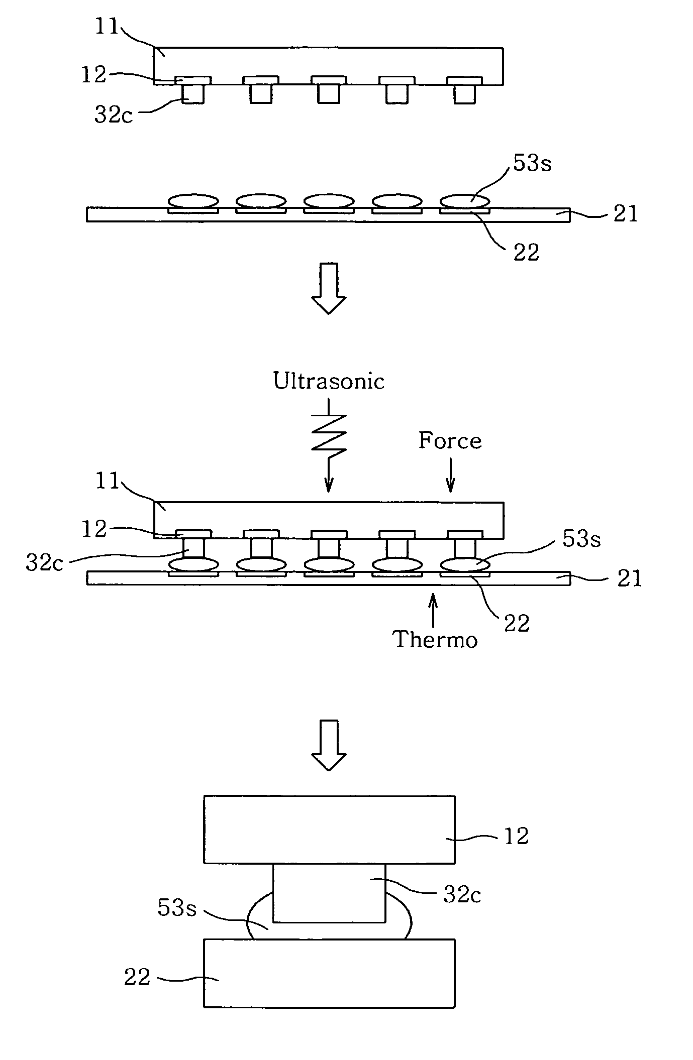
[0066]FIG. 29 is a view showing the process for a flip chip bonding between a substrate that is formed with a stud bump and a chip that is formed with a plated bump using a thermosonic method according to the invention.

[0067]Referring to FIG. 29, an aluminum bonding pad 12 of a chip 11 is formed with a plated bump 32c that is made of Au, Al, or Ni coated with Au. A lead pad 22 of a substrate 21 is formed with a stud bump 53s that is made of Au or Cu. In the flip chip bonding process S5, after the chip 11 and the substrate 21 are closely contacted, heat is applied to the substrate 21, and an ultrasonic wave of 70 KHz or more is applied to the chip 11 through a collet 95. Simultaneously, pressure is applied to the substrate 21. As a result, the plated bump 32c of the chip and the stud bump 53s of the substrate are bonded by energy generated from the heat, the ultrasonic wave and the pressure. Here, the collet 95 that is made of Zr, Ti, ceramic, stainless alloy, TiW alloy, TiC, and the...

example 2

[0068]FIG. 30 is a view showing the process for a flip chip bonding between a bare substrate and a chip that is formed with a plated bump u sing a thermosonic method according to the invention.

[0069]Referring to FIG. 30, an aluminum bonding pad 12 of a chip 11 is formed with a plated bump 32c that is made of Au, Al, or Ni coated with Au. A lead pad 22 of a substrate 21 is bare of any bump. In the flip chip bonding process S5, after the chip 11 and the substrate 21 are closely contacted, heat is applied to the substrate 21, and an ultrasonic wave is applied to the chip 11 through a collet 95. Simultaneously, pressure is applied to the substrate 21. As a result, the plated bump 32c of the chip and the lead pad 22 of the substrate are bonded by energy generated from the heat, the ultrasonic wave and the pressure.

example 3

[0070]FIG. 31 is a view showing the process for a flip chip bonding between a substrate that is formed with a stud bump and a chip that is formed with a plated bump and a stud bump formed on the plated bump using a thermosonic method according to the invention.

[0071]Referring to FIG. 31, an aluminum bonding pad 12 of a chip 11 is formed with a plated bump 32c that is made of Au, Al, Ag, Cu or Ni coated with Au. A stud bump 53c is again formed on the plated bump 32c. A lead pad 22 of a substrate 21 is formed with a stud bump 53s. In the flip chip bonding process S5, after the chip 11 and the substrate 21 are closely contacted, heat is applied to the substrate 21, and an ultrasonic wave of 70 KHz or more is applied to the chip 11 through a collet 95. Simultaneously, pressure is applied to the substrate 21. As a result, the stud bump 53c of the chip 11 and the stud bump 53s of the substrate are bonded by energy generated from the heat, the ultrasonic wave of 70 KHz or more and the pres...


PUM

PropertyMeasurementUnit
thicknessaaaaaaaaaa
thicknessaaaaaaaaaa
pressureaaaaaaaaaa

Abstract

A flip chip bonding method and substrate architecture are disclosed for enhancing bonding performance between a chip and a substrate by forming a bump on the chip or the substrate. The flip chip bonding method includes performing pretreatment of a wafer having chips, dicing, and obtaining the pretreated individual chip; performing pretreatment of a substrate; aligning the pads of the pretreated chip with the pads of the pretreated substrate, and bonding the chip and the substrate together by applying an ultrasonic wave and heat using a collet and simultaneously applying pressure. Post treatment is performed by filling or molding resin after bonding. The chip or the substrate is formed with a plated bump, a stud bump or a wedge bump. The stud bump or the wedge bump can be additionally formed on the plated bump.

Description

TECHNICAL FIELD[0001]This invention relates to a semiconductor packaging technology, and more particularly to a flip chip bonding method for enhancing a bonding performance between a chip and a substrate by forming a bump on the chip, the substrate, or both the chip and the substrate and for bonding the chip and the substrate using a thermosonic process, and a layer-built structure of the substrate for the same.BACKGROUND ART[0002]Generally, a wire bonding, a TAP bonding, a flip chip bonding, and the like have been disclosed as methods for bonding a semiconductor chip to a substrate. Meanwhile, the size of an electronic product is gradually minimized, and its performance is more enhanced. The number of bonding pads for input and output has increased, while the size of the chip used in the electronic product has gradually become smaller. Thus, the conventional wire bonding process for bonding the semiconductor chip on the substrate has arrived at its limit. Instead of the wire bondin...

Claims


Application Information

Patent Timeline
Patent Type & Authority Patents(United States)
IPC IPC(8): H01L21/44H01L21/56H01L21/60
CPCH01L21/563H01L24/11H01L24/31H01L24/81H01L24/29H01L2224/1134H01L2224/13099H01L2224/13144H01L2224/13147H01L2224/16145H01L2224/16225H01L2224/48095H01L2224/48465H01L2224/73203H01L2224/81801H01L2224/81894H01L2224/83192H01L2224/83951H01L2924/01005H01L2924/01013H01L2924/01022H01L2924/01029H01L2924/01033H01L2924/0104H01L2924/01046H01L2924/01047H01L2924/0105H01L2924/01057H01L2924/01058H01L2924/01074H01L2924/01078H01L2924/01079H01L2924/01082H01L2924/01327H01L2924/09701H01L2924/15311H01L2924/16195H01L2924/01006H01L2924/014H01L2224/32145H01L2224/73204H01L2224/45124H01L2224/45144H01L2224/45147H01L2224/32225H01L24/45H01L2224/45139H01L2924/07811H01L2924/07802H01L2924/00014H01L2924/00H01L2924/181H01L2924/12042H01L2224/05571H01L2224/05573H01L2224/48463H01L2224/81207H01L2224/05624H01L24/05H01L24/13H01L24/16H01L2224/81191H01L2224/81193H01L2224/73207H01L2224/45015H01L2924/207H01L21/60H01L2224/05124
Inventor KOO, JA UKKIM, HYOUNG CHAN
Owner KOO JA UK
Why Eureka
Try Eureka