Single supply level converter

a level converter and single supply technology, applied in logic circuits, pulse automatic control, pulse techniques, etc., can solve the problems of power consumption, chip power consumption has increased, cooling and packaging costs have increased, etc., and achieve the effect of reducing the power of the level converter

Active Publication Date: 2006-10-10
MEDIATEK INC
View PDF5 Cites 28 Cited by
  • Summary
  • Abstract
  • Description
  • Claims
  • Application Information

AI Technical Summary

Benefits of technology

[0017]The present invention relates to a level converter for interfacing two circuits supplied by different supply voltages, and integrated circuit including the level converter interfacing circuits in two different voltage islands. A first buffer is supplied by a virtual supply and receives an input signal from a lower voltage circuit. The first buffer drives a second buffer, which is supplied by a higher supply voltage. An output from the second buffer switches a supply select to selectively pass the higher supply voltage or a reduced supply voltage to the first buffer.

Problems solved by technology

Thus, not withstanding the decrease of chip supply voltage, chip power consumption has increased as well.
Both at the chip and system levels, cooling and packaging costs have escalated as a natural result of this increase in chip power.
Consequently, power consumption has been a major design consideration for designing very large scale integrated circuits (VLSI) such as high performance microprocessors.
In particular, increasing power requirements run counter to the low end design goal of longer battery life.
While reducing supply voltage is attractive to reduce the power consumption, reducing Vdd increases transistor and gate delay.
However, it is often the case that most cells in a chip are timing non-critical.
Unfortunately, level converters add to overhead, increasing chip power and each takes up space decreasing area available for other circuits.
This complicates the physical design for multiple supply voltage circuits because the level converters can only be physically placed in regions which have access to both power supplies.
In addition, due to the differential nature of the traditional level converter circuits, the power consumption by the level converter circuits can significantly offset any power reduction possible realized by migrating to a multiple supply voltage design.
Also, since these level converters add delay, this additional delay may prevent switching some circuits to the lower supply voltage, further offsetting power reduction that would otherwise be realized.
Also, these differential level converters are not easily adaptable for other logic functions than a simple buffer or inverter, which might otherwise provide additional savings in delay and power.

Method used


Image

  • Single supply level converter
  • Single supply level converter
  • Single supply level converter

Examples


Embodiment Construction

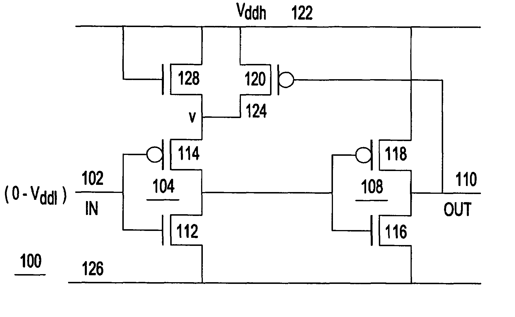
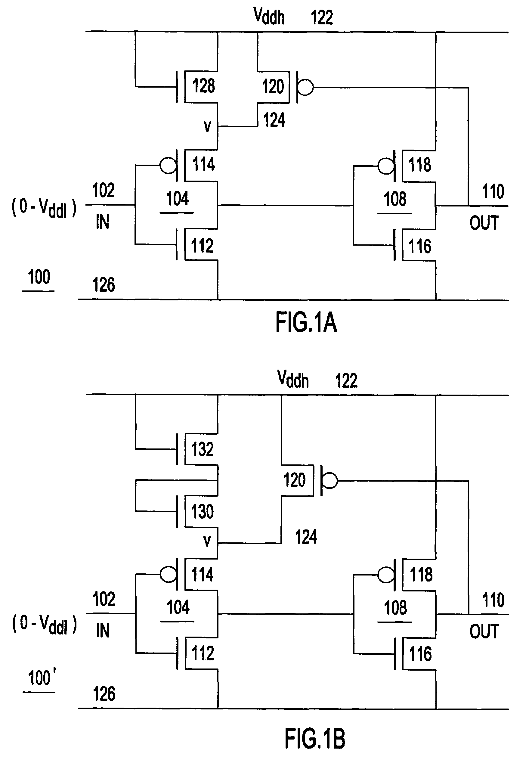
[0024]Turning now to the drawings and more particularly, FIGS. 1A–B show examples of simple single supply level converters 100, 100′, receiving a low supply voltage signal at input 102 according to a preferred embodiment of the present invention. Essentially, in this example, each level converter 100, 100′ is a pair of series connected buffers (inverters 104 and 108 in this example) with the output 110 of the second inverter 108 switching the supply voltage for the input inverter 104. Each input inverter 104 includes a pair of series connected complementary field effect transistors (FETs) n-type FET (NFET) 112 and p-type FET (PFET) 114. Input 102 receives a low voltage signal and drives the gates of NFET 112 and PFET 114. The second inverter 108 also includes a pair of series connected devices, NFET 116 and PFET 118, which are connected together at their drains at output 110. The drains of NFET 112 and PFET 114 are connected together forming the output of the first inverter 104, whi...


PUM


Abstract

A level converter for interfacing two circuits supplied by different supply voltages, and integrated circuit including the level converter interfacing circuit in two different voltage islands. A first buffer is supplied by a virtual supply and receives an input signal from a lower voltage circuit. The first buffer drives a second buffer, which is supplied by a higher supply voltage. An output from the second buffer switches a supply select to selectively pass the higher supply voltage or a reduced supply voltage to the first buffer.

Description

CROSS REFERENCE TO RELATED APPLICATION[0001]The present invention is related to U.S. application Ser. No. 10 / 720,464 entitled “MULTIPLE VOLTAGE INTEGRATED CIRCUIT AND DESIGN METHOD THEREFOR” to Anthony Correale Jr. et al., U.S. application Ser. No. 10 / 720,562 entitled “METHOD AND PROGRAM PRODUCT OF LEVEL CONVERTER OPTIMIZATION” to Anthony Correale Jr. et al., both filed coincident herewith and to U.S. application Ser. No. 10 / 387,728 entitled “VOLTAGE ISLAND CIRCUIT PLACEMENT” to Anthony Correale Jr., filed Mar. 13, 2003, all assigned to the assignee of the present invention.BACKGROUND OF THE INVENTION[0002]1. Field of the Invention[0003]The present invention is related to integrated circuit (IC) design and more particularly, to optimizing standard cell design configurations.[0004]2. Background Description[0005]Semiconductor technology and chip manufacturing advances have resulted in a steady increase of on-chip clock frequencies, the number of transistors on a single chip and the di...

Claims


Application Information

Patent Timeline
Patent Type & Authority Patents(United States)
IPC IPC(8): H03K19/0175H03K19/094H03K19/0185H03K19/0948
CPCH03K19/018521H03K19/0948
Inventor CORREALE, JR., ANTHONYJOSHI, RAJIV V.KUNG, DAVID S.PAN, ZHIGANGPURI, RUCHIR
Owner MEDIATEK INC
Why Eureka
Try Eureka